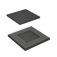
HD6417720BP133BV Renesas Electronics America, HD6417720BP133BV Datasheet - Page 54

HD6417720BP133BV
Manufacturer Part Number
HD6417720BP133BV
Description
SH3-DSP, WITH USB AND LCDC, PB-F
Manufacturer
Renesas Electronics America
Series
SuperH® SH7700r
Datasheet
1.R8A77210C133BAV.pdf
(1478 pages)
Specifications of HD6417720BP133BV
Core Processor
SH-3 DSP
Core Size
32-Bit
Speed
133MHz
Connectivity
FIFO, I²C, IrDA, MMC, SCI, SD, SIO, SIM, USB
Peripherals
DMA, LCD, POR, WDT
Number Of I /o
117
Program Memory Type
ROMless
Ram Size
16K x 8
Voltage - Supply (vcc/vdd)
1.4 V ~ 1.6 V
Data Converters
A/D 4x10b; D/A 2x8b
Oscillator Type
Internal
Operating Temperature
-20°C ~ 75°C
Package / Case
256-BGA
Lead Free Status / RoHS Status
Lead free / RoHS Compliant
Eeprom Size
-
Program Memory Size
-
- Current page: 54 of 1478
- Download datasheet (10Mb)
Table 9.13
Table 9.14
Table 9.15
Table 9.15
Table 9.16
Table 9.16
Table 9.17
Table 9.17
Table 9.18
Table 9.19
Table 9.20
Table 9.21
Section 10 Direct Memory Access Controller (DMAC)
Table 10.1
Table 10.2
Table 10.3
Table 10.4
Table 10.5
Table 10.6
Table 10.7
Table 10.8
Section 11 Clock Pulse Generator (CPG)
Table 11.1
Table 11.2
Table 11.3
Section 13 Power-Down Modes
Table 13.1
Table 13.2
Page liv of lx
Relationship between A2/3BSZ[1:0], A2/3ROW[1:0], A2/3COL[1:0],
and Address Multiplex Output (2)-2..................................................................... 352
Relationship between A2/3BSZ[1:0], A2/3ROW[1:0], A2/3COL[1:0],
and Address Multiplex Output (3) ........................................................................ 353
Relationship between A2/3BSZ[1:0], A2/3ROW[1:0], A2/3COL[1:0],
and Address Multiplex Output (4)-1..................................................................... 354
Relationship between A2/3BSZ[1:0], A2/3ROW[1:0], A2/3COL[1:0],
and Address Multiplex Output (4)-2..................................................................... 355
Relationship between A2/3BSZ[1:0], A2/3ROW[1:0], A2/3COL[1:0],
and Address Multiplex Output (5)-1..................................................................... 356
Relationship between A2/3BSZ[1:0], A2/3ROW[1:0], A2/3COL[1:0],
and Address Multiplex Output (5)-2..................................................................... 357
Relationship between A2/3BSZ[1:0], A2/3ROW[1:0], A2/3COL[1:0],
and Address Multiplex Output (6)-1..................................................................... 358
Relationship between A2/3BSZ[1:0], A2/3ROW[1:0], A2/3COL[1:0],
and Address Multiplex Output (6)-2..................................................................... 359
Relationship between Access Size and Number of Bursts.................................... 360
Access Address in SDRAM Mode Register Write ............................................... 380
Output Addresses when EMRS Command is Issued ............................................ 383
Relationship between Bus Width, Access Size, and Number of Bursts................ 386
Pin Configuration.................................................................................................. 409
Transfer Request Sources ..................................................................................... 423
Selecting External Request Modes with RS Bits .................................................. 426
Selecting External Request Detection with DL, DS Bits ...................................... 427
Selecting External Request Detection with DO Bit .............................................. 427
Selecting On-Chip Peripheral Module Request Modes with RS3 to RS0 Bits ..... 429
Supported DMA Transfers.................................................................................... 434
Relationship between Request Modes and Bus Modes
by DMA Transfer Category.................................................................................. 441
Pin Configuration.................................................................................................. 459
Clock Operating Modes ........................................................................................ 460
Possible Combination of Clock Mode and FRQCR Values ................................. 461
States of Power-Down Modes .............................................................................. 480
Pin Configuration.................................................................................................. 481
R01UH0083EJ0400 Rev. 4.00
Sep 21, 2010
Related parts for HD6417720BP133BV
Image
Part Number
Description
Manufacturer
Datasheet
Request
R

Part Number:
Description:
KIT STARTER FOR M16C/29
Manufacturer:
Renesas Electronics America
Datasheet:

Part Number:
Description:
KIT STARTER FOR R8C/2D
Manufacturer:
Renesas Electronics America
Datasheet:

Part Number:
Description:
R0K33062P STARTER KIT
Manufacturer:
Renesas Electronics America
Datasheet:

Part Number:
Description:
KIT STARTER FOR R8C/23 E8A
Manufacturer:
Renesas Electronics America
Datasheet:

Part Number:
Description:
KIT STARTER FOR R8C/25
Manufacturer:
Renesas Electronics America
Datasheet:

Part Number:
Description:
KIT STARTER H8S2456 SHARPE DSPLY
Manufacturer:
Renesas Electronics America
Datasheet:

Part Number:
Description:
KIT STARTER FOR R8C38C
Manufacturer:
Renesas Electronics America
Datasheet:

Part Number:
Description:
KIT STARTER FOR R8C35C
Manufacturer:
Renesas Electronics America
Datasheet:

Part Number:
Description:
KIT STARTER FOR R8CL3AC+LCD APPS
Manufacturer:
Renesas Electronics America
Datasheet:

Part Number:
Description:
KIT STARTER FOR RX610
Manufacturer:
Renesas Electronics America
Datasheet:

Part Number:
Description:
KIT STARTER FOR R32C/118
Manufacturer:
Renesas Electronics America
Datasheet:

Part Number:
Description:
KIT DEV RSK-R8C/26-29
Manufacturer:
Renesas Electronics America
Datasheet:

Part Number:
Description:
KIT STARTER FOR SH7124
Manufacturer:
Renesas Electronics America
Datasheet:

Part Number:
Description:
KIT STARTER FOR H8SX/1622
Manufacturer:
Renesas Electronics America
Datasheet:

Part Number:
Description:
KIT DEV FOR SH7203
Manufacturer:
Renesas Electronics America
Datasheet:


