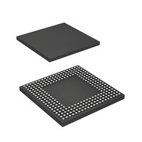
HD6417720BP133BV Renesas Electronics America, HD6417720BP133BV Datasheet - Page 1010

HD6417720BP133BV
Manufacturer Part Number
HD6417720BP133BV
Description
SH3-DSP, WITH USB AND LCDC, PB-F
Manufacturer
Renesas Electronics America
Series
SuperH® SH7700r
Datasheet
1.R8A77210C133BAV.pdf
(1478 pages)
Specifications of HD6417720BP133BV
Core Processor
SH-3 DSP
Core Size
32-Bit
Speed
133MHz
Connectivity
FIFO, I²C, IrDA, MMC, SCI, SD, SIO, SIM, USB
Peripherals
DMA, LCD, POR, WDT
Number Of I /o
117
Program Memory Type
ROMless
Ram Size
16K x 8
Voltage - Supply (vcc/vdd)
1.4 V ~ 1.6 V
Data Converters
A/D 4x10b; D/A 2x8b
Oscillator Type
Internal
Operating Temperature
-20°C ~ 75°C
Package / Case
256-BGA
Lead Free Status / RoHS Status
Lead free / RoHS Compliant
Eeprom Size
-
Program Memory Size
-
- Current page: 1010 of 1478
- Download datasheet (10Mb)
Section 27 A/D Converter
27.7.6
Operating the chip in excess of the following voltage range may result in damage to chip
reliability.
During A/D conversion, the voltages (VANn) input to the analog input pins ANn should be in the
range AV
27.7.7
In designing a board, separate digital circuits and analog circuits. Do not intersect or locate closely
signal lines of a digital circuit and an analog circuit. An analog circuit may malfunction due to
induction, thus affecting A/D conversion values. Separate analog input pins (AN0 to AN3) and the
analog power voltage (AVcc) from digital circuits with analog ground (AVss). Connect analog
ground (AVss) to one point of stable ground (Vss) on the board.
27.7.8
Connect a protective circuit between AVcc and AVss, as shown in figure 27.9, to prevent damage
of analog input pins (AN0 to AN3) due to abnormal voltage such as excessive serge. Connect a
bypass capacitor that is connected to AVcc and a capacitor for a filter that is connected to AN0 to
AN3 to AVss.
When a capacitor for a filter is connected, input currents of AN0 to AN3 are averaged, may
causing errors. If A/D conversion is frequently performed in scan mode, voltages of analog input
pins cause errors when a current that is charged/discharged for capacitance of a sample & hold
circuit in the A/D converter is higher than a current that is input through input impedance (Rin).
Therefore, determine a circuit constant carefully.
Page 950 of 1414
Setting Analog Input Voltage
Notes on Board Design
Notes on Countermeasures to Noise
SS
≤ VANn ≤ AV
CC
(n = 0 to 3).
SH7720 Group, SH7721 Group
R01UH0083EJ0400 Rev. 4.00
Sep 21, 2010
Related parts for HD6417720BP133BV
Image
Part Number
Description
Manufacturer
Datasheet
Request
R

Part Number:
Description:
KIT STARTER FOR M16C/29
Manufacturer:
Renesas Electronics America
Datasheet:

Part Number:
Description:
KIT STARTER FOR R8C/2D
Manufacturer:
Renesas Electronics America
Datasheet:

Part Number:
Description:
R0K33062P STARTER KIT
Manufacturer:
Renesas Electronics America
Datasheet:

Part Number:
Description:
KIT STARTER FOR R8C/23 E8A
Manufacturer:
Renesas Electronics America
Datasheet:

Part Number:
Description:
KIT STARTER FOR R8C/25
Manufacturer:
Renesas Electronics America
Datasheet:

Part Number:
Description:
KIT STARTER H8S2456 SHARPE DSPLY
Manufacturer:
Renesas Electronics America
Datasheet:

Part Number:
Description:
KIT STARTER FOR R8C38C
Manufacturer:
Renesas Electronics America
Datasheet:

Part Number:
Description:
KIT STARTER FOR R8C35C
Manufacturer:
Renesas Electronics America
Datasheet:

Part Number:
Description:
KIT STARTER FOR R8CL3AC+LCD APPS
Manufacturer:
Renesas Electronics America
Datasheet:

Part Number:
Description:
KIT STARTER FOR RX610
Manufacturer:
Renesas Electronics America
Datasheet:

Part Number:
Description:
KIT STARTER FOR R32C/118
Manufacturer:
Renesas Electronics America
Datasheet:

Part Number:
Description:
KIT DEV RSK-R8C/26-29
Manufacturer:
Renesas Electronics America
Datasheet:

Part Number:
Description:
KIT STARTER FOR SH7124
Manufacturer:
Renesas Electronics America
Datasheet:

Part Number:
Description:
KIT STARTER FOR H8SX/1622
Manufacturer:
Renesas Electronics America
Datasheet:

Part Number:
Description:
KIT DEV FOR SH7203
Manufacturer:
Renesas Electronics America
Datasheet:


