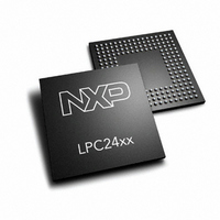
LPC2468FET208,551 NXP Semiconductors, LPC2468FET208,551 Datasheet - Page 713

LPC2468FET208,551
Manufacturer Part Number
LPC2468FET208,551
Description
IC ARM7 MCU FLASH 512K 208TFBGA
Manufacturer
NXP Semiconductors
Series
LPC2400r
Specifications of LPC2468FET208,551
Program Memory Type
FLASH
Program Memory Size
512KB (512K x 8)
Package / Case
208-TFBGA
Core Processor
ARM7
Core Size
16/32-Bit
Speed
72MHz
Connectivity
CAN, EBI/EMI, Ethernet, I²C, Microwire, MMC, SPI, SSI, SSP, UART/USART, USB OTG
Peripherals
Brown-out Detect/Reset, DMA, I²S, POR, PWM, WDT
Number Of I /o
160
Ram Size
98K x 8
Voltage - Supply (vcc/vdd)
3 V ~ 3.6 V
Data Converters
A/D 8x10b; D/A 1x10b
Oscillator Type
Internal
Operating Temperature
-40°C ~ 85°C
Processor Series
LPC24
Core
ARM7TDMI-S
Data Bus Width
16 bit, 32 bit
Data Ram Size
98 KB
Interface Type
CAN/I2S/ISP/SSP/UART/USB
Maximum Clock Frequency
72 MHz
Number Of Programmable I/os
160
Number Of Timers
6
Operating Supply Voltage
3.3 V
Maximum Operating Temperature
+ 85 C
Mounting Style
SMD/SMT
3rd Party Development Tools
MDK-ARM, RL-ARM, ULINK2, IRD-LPC2468-DEV, SAB-TFBGA208, KSK-LPC2468-PL
Development Tools By Supplier
OM10100
Minimum Operating Temperature
- 40 C
On-chip Adc
8-ch x 10-bit
On-chip Dac
1-ch x 10-bit
Package
208TFBGA
Device Core
ARM7TDMI-S
Family Name
LPC2000
Maximum Speed
72 MHz
Lead Free Status / RoHS Status
Lead free / RoHS Compliant
For Use With
622-1025 - KIT DEV IND REF DESIGN LPC2468622-1024 - BOARD SCKT ADAPTER FOR TFBGA208568-4358 - DISPLAY QVGA TFT FOR OM10100568-4309 - BOARD EXTENSION LPCSTICK568-4308 - EVAL LPC-STICK WITH LPC2468MCB2400U - BOARD EVAL MCB2400 + ULINK2MCB2400 - BOARD EVAL FOR NXP LPC246X SER622-1005 - USB IN-CIRCUIT PROG ARM7 LPC2K
Eeprom Size
-
Lead Free Status / Rohs Status
Lead free / RoHS Compliant
Other names
568-4262
935283234551
LPC2468FET208-S
935283234551
LPC2468FET208-S
Available stocks
Company
Part Number
Manufacturer
Quantity
Price
Company:
Part Number:
LPC2468FET208,551
Manufacturer:
NXP
Quantity:
6 174
Company:
Part Number:
LPC2468FET208,551
Manufacturer:
NXP Semiconductors
Quantity:
10 000
- Current page: 713 of 792
- Download datasheet (5Mb)
NXP Semiconductors
UM10237_4
User manual
Fig 144. GPDMA block diagram
4.2.1 AHB Slave Interface
4.2.2 Control Logic and Register Bank
4.2.3 DMA Request and Response Interface
responses
Interrupts
requests
AHB BUS
DMA
DMA
DMA
example, a bidirectional port requires one stream for transmit and one for receive. The
source and destination areas can each be either a memory region or a peripheral, and
can be accessed through the AHB master.
Figure 32–144
The functions of the GPDMA are described in the following sections:
All transactions on the AHB slave programming bus of the GPDMA are 32 bit wide.
The register block stores data written, or to be read across the AHB interface.
See DMA Interface description for information on the DMA request and response
interface.
•
•
•
•
•
•
•
•
AHB slave interface
Control logic and register bank
DMA request and response interface
Channel logic and channel register bank
Interrupt request
AHB master interface
Channel hardware
DMA request priority
INTERFACE
INTERFACE
INTERRUPT
AHB SLAVE
RESPONSE
REQUEST
REQUEST
DMA
AND
shows a block diagram of the GPDMA.
Chapter 32: LPC24XX General Purpose DMA (GPDMA) controller
Rev. 04 — 26 August 2009
REGISTERS
REGISTERS
LOGIC AND
LOGIC AND
CONTROL
CHANNEL
GPDMA
INTERFACE
MASTER
AHB
AHB BUS
UM10237
© NXP B.V. 2009. All rights reserved.
713 of 792
Related parts for LPC2468FET208,551
Image
Part Number
Description
Manufacturer
Datasheet
Request
R
Part Number:
Description:
NXP Semiconductors designed the LPC2468 microcontroller around a 16-bit/32-bitARM7TDMI-S CPU core with real-time debug interfaces that include both JTAG andembedded trace
Manufacturer:
NXP Semiconductors
Datasheet:

Part Number:
Description:
MCU, MPU & DSP Development Tools Ind. Ref. Design LPC2468 Dev Kit V1.2
Manufacturer:
FDI
Datasheet:

Part Number:
Description:
MCU, MPU & DSP Development Tools KICKSTART KIT NXP LPC2468
Manufacturer:
IAR Systems

Part Number:
Description:
MCU, MPU & DSP Development Tools DEV BRD FOR LPC2468 128MBFLASH 16MBSDRAM
Manufacturer:
Olimex Ltd.
Datasheet:

Part Number:
Description:
MCU, MPU & DSP Development Tools LPC2468 OEM BRD OEM BASE BRD BUNDLE
Manufacturer:
Embedded Artists
Part Number:
Description:
Lpc2468 Single-chip 16-bit/32-bit Micro; 512 Kb Flash, Ethernet, Can, Isp/iap, Usb 2.0 Device/host/otg, External Memory Interface
Manufacturer:
NXP Semiconductors
Datasheet:
Part Number:
Description:
NXP Semiconductors designed the LPC2420/2460 microcontroller around a 16-bit/32-bitARM7TDMI-S CPU core with real-time debug interfaces that include both JTAG andembedded trace
Manufacturer:
NXP Semiconductors
Datasheet:

Part Number:
Description:
NXP Semiconductors designed the LPC2458 microcontroller around a 16-bit/32-bitARM7TDMI-S CPU core with real-time debug interfaces that include both JTAG andembedded trace
Manufacturer:
NXP Semiconductors
Datasheet:
Part Number:
Description:
NXP Semiconductors designed the LPC2470 microcontroller, powered by theARM7TDMI-S core, to be a highly integrated microcontroller for a wide range ofapplications that require advanced communications and high quality graphic displays
Manufacturer:
NXP Semiconductors
Datasheet:
Part Number:
Description:
NXP Semiconductors designed the LPC2478 microcontroller, powered by theARM7TDMI-S core, to be a highly integrated microcontroller for a wide range ofapplications that require advanced communications and high quality graphic displays
Manufacturer:
NXP Semiconductors
Datasheet:
Part Number:
Description:
The Philips Semiconductors XA (eXtended Architecture) family of 16-bit single-chip microcontrollers is powerful enough to easily handle the requirements of high performance embedded applications, yet inexpensive enough to compete in the market for hi
Manufacturer:
NXP Semiconductors
Datasheet:
Part Number:
Description:
The XA-S3 device is a member of Philips Semiconductors? XA(eXtended Architecture) family of high performance 16-bitsingle-chip microcontrollers
Manufacturer:
NXP Semiconductors
Datasheet:

Part Number:
Description:
The NXP BlueStreak LH75401/LH75411 family consists of two low-cost 16/32-bit System-on-Chip (SoC) devices
Manufacturer:
NXP Semiconductors
Datasheet:

Part Number:
Description:
The NXP LPC3130/3131 combine an 180 MHz ARM926EJ-S CPU core, high-speed USB2
Manufacturer:
NXP Semiconductors
Datasheet:


