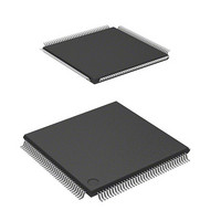
DF2117VT20V Renesas Electronics America, DF2117VT20V Datasheet - Page 1010

DF2117VT20V
Manufacturer Part Number
DF2117VT20V
Description
MCU 16BIT FLASH 3V 160K 144-TQFP
Manufacturer
Renesas Electronics America
Series
H8® H8S/2100r
Datasheet
1.DF2117VT20HV.pdf
(1040 pages)
Specifications of DF2117VT20V
Core Processor
H8S/2600
Core Size
16-Bit
Speed
20MHz
Connectivity
FIFO, I²C, LPC, SCI, SmartCard
Peripherals
POR, PWM, WDT
Number Of I /o
112
Program Memory Size
160KB (160K x 8)
Program Memory Type
FLASH
Ram Size
8K x 8
Voltage - Supply (vcc/vdd)
3 V ~ 3.6 V
Data Converters
A/D 16x10b
Oscillator Type
External
Operating Temperature
-20°C ~ 75°C
Package / Case
144-TQFP, 144-VQFP
Lead Free Status / RoHS Status
Lead free / RoHS Compliant
Eeprom Size
-
Available stocks
Company
Part Number
Manufacturer
Quantity
Price
Company:
Part Number:
DF2117VT20V
Manufacturer:
Renesas
Quantity:
100
Company:
Part Number:
DF2117VT20V
Manufacturer:
Renesas Electronics America
Quantity:
10 000
- Current page: 1010 of 1040
- Download datasheet (7Mb)
28.3.3
Table 28.7 shows the on-chip peripheral module timing. The on-chip peripheral modules that can
be operated by the subclock (φ = 32.768 kHz) are I/O ports, external interrupts (NMI, IRQ0 to
IRQ15, KIN0 to KIN15, WUE8 to WUE15, and KBCA to KBCD) and watchdog timer (WDT_1)
only. The system clock or LCLK operation can be used in the FSI.
Table 28.7 Timing of On-Chip Peripheral Modules
Conditions:
Rev. 2.00 Sep. 28, 2009 Page 968 of 994
REJ09B0452-0200
Item
I/O ports
TPU
TMR
TCM
TDP
PWMU, PWMX
SCI
Timing of On-Chip Peripheral Modules
V
operating frequency, FSICK = 8 MHz to maximum operating frequency or LCLK
(33 MHz)
Output data delay time*
Input data setup time
Input data hold time
Timer output delay time
Timer input setup time
Timer clock input setup time
Timer clock
pulse width
Timer output delay time
Timer reset input setup time
Timer clock input setup time
Timer clock
pulse width
TCM input setup time
TCM clock input setup time
TCM clock pulse width
TDP input setup time
TDP clock input setup time
TDP clock pulse width
Pulse output delay time
Input clock cycle
Input clock pulse width
CC
= 3.0 V to 3.6 V, V
Single edge
Both edges
Single edge
Both edges
Asynchronous
Synchronous
2
SS
= 0 V, φ = 32.768 kHz*
Symbol
t
t
t
t
t
t
t
t
t
t
t
t
t
t
t
t
t
t
t
t
t
t
PWD
PRS
PRH
TOCD
TICS
TCKS
TCKWH
TCKWL
TMOD
TMRS
TMCS
TMCWH
TMCWL
TCMS
TCMCKS
TCMCKW
TDPS
TDPCKS
TDPCKW
PWOD
Scyc
SCKW
Min.
⎯
30
30
⎯
30
30
1.5
2.5
⎯
30
30
1.5
2.5
30
30
1.5
30
30
1.5
⎯
4
6
0.4
1
, φ = 8 MHz to maximum
Max.
50
⎯
⎯
50
⎯
⎯
⎯
⎯
50
⎯
⎯
⎯
⎯
⎯
⎯
⎯
⎯
⎯
⎯
50
⎯
⎯
0.6
Unit
ns
ns
t
ns
t
ns
t
ns
t
ns
t
t
cyc
cyc
cyc
cyc
cyc
Scyc
Test
Conditions
Figure 28.9
Figure 28.10
Figure 28.11
Figure 28.12
Figure 28.14
Figure 28.13
Figure 28.15
Figure 28.16
Figure 28.17
Figure 28.18
Figure 28.19
Figure 28.20
Related parts for DF2117VT20V
Image
Part Number
Description
Manufacturer
Datasheet
Request
R

Part Number:
Description:
0.6mm Pitch Board-to-Fine-Coaxial Cable Connectors
Manufacturer:
Hirose Electric
Datasheet:

Part Number:
Description:
0.6mm Pitch Board-to-fine-coaxial Cable Connectors
Manufacturer:
Hirose Electric
Datasheet:

Part Number:
Description:
0.6mm Pitch Board-to-fine-coaxial Cable Connectors
Manufacturer:
Hirose Electric
Datasheet:

Part Number:
Description:
Right angle, Two-piece for fine coaxial cable, Discrete wire connectors; HRS No: 687-0001-5 56; No. of Positions: 20; Connector Type: Board mounting; Contact Gender: Female; Contact Spacing (mm): 0.6; Terminal Pitch (mm): 0.6; PCB Mount Type: SMT; Cu
Manufacturer:
Hirose Electric

Part Number:
Description:
0.6mm Pitch Board-to-fine-coaxial Cable Connectors
Manufacturer:
Hirose Electric
Datasheet:

Part Number:
Description:
0.6mm Pitch Board-to-Fine-Coaxial Cable Connectors
Manufacturer:
HIROSE [Hirose Electric]
Datasheet:

Part Number:
Description:
KIT STARTER FOR M16C/29
Manufacturer:
Renesas Electronics America
Datasheet:

Part Number:
Description:
KIT STARTER FOR R8C/2D
Manufacturer:
Renesas Electronics America
Datasheet:

Part Number:
Description:
R0K33062P STARTER KIT
Manufacturer:
Renesas Electronics America
Datasheet:

Part Number:
Description:
KIT STARTER FOR R8C/23 E8A
Manufacturer:
Renesas Electronics America
Datasheet:

Part Number:
Description:
KIT STARTER FOR R8C/25
Manufacturer:
Renesas Electronics America
Datasheet:

Part Number:
Description:
KIT STARTER H8S2456 SHARPE DSPLY
Manufacturer:
Renesas Electronics America
Datasheet:

Part Number:
Description:
KIT STARTER FOR R8C38C
Manufacturer:
Renesas Electronics America
Datasheet:

Part Number:
Description:
KIT STARTER FOR R8C35C
Manufacturer:
Renesas Electronics America
Datasheet:

Part Number:
Description:
KIT STARTER FOR R8CL3AC+LCD APPS
Manufacturer:
Renesas Electronics America
Datasheet:


