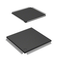
DF2117VT20V Renesas Electronics America, DF2117VT20V Datasheet - Page 835

DF2117VT20V
Manufacturer Part Number
DF2117VT20V
Description
MCU 16BIT FLASH 3V 160K 144-TQFP
Manufacturer
Renesas Electronics America
Series
H8® H8S/2100r
Datasheet
1.DF2117VT20HV.pdf
(1040 pages)
Specifications of DF2117VT20V
Core Processor
H8S/2600
Core Size
16-Bit
Speed
20MHz
Connectivity
FIFO, I²C, LPC, SCI, SmartCard
Peripherals
POR, PWM, WDT
Number Of I /o
112
Program Memory Size
160KB (160K x 8)
Program Memory Type
FLASH
Ram Size
8K x 8
Voltage - Supply (vcc/vdd)
3 V ~ 3.6 V
Data Converters
A/D 16x10b
Oscillator Type
External
Operating Temperature
-20°C ~ 75°C
Package / Case
144-TQFP, 144-VQFP
Lead Free Status / RoHS Status
Lead free / RoHS Compliant
Eeprom Size
-
Available stocks
Company
Part Number
Manufacturer
Quantity
Price
Company:
Part Number:
DF2117VT20V
Manufacturer:
Renesas
Quantity:
100
Company:
Part Number:
DF2117VT20V
Manufacturer:
Renesas Electronics America
Quantity:
10 000
- Current page: 835 of 1040
- Download datasheet (7Mb)
Except for MAT switching, the erasing procedure is the same as that in user program mode.
The area that can be executed in the steps of the user procedure program (on-chip RAM and user
MAT) is shown in section 24.8.4, Storable Areas for On-Chip Program and Program Data.
24.8.4
In the descriptions in this manual, the on-chip programs and program data storage areas are
assumed to be in the on-chip RAM. However, they can be executed from part of the flash memory
which is not to be programmed or erased as long as the following conditions are satisfied.
• The on-chip program is downloaded to and executed in the on-chip RAM specified by
• Since the on-chip program uses a stack area, allocate 128 bytes at the maximum as a stack
• Download requested by setting the SCO bit in FCCS to 1 should be executed from the on-chip
• In an operating mode in which the external address space is not accessible, such as single-chip
• The flash memory is not accessible during programming/erasing. Programming/erasing is
• After programming/erasing starts, access to the flash memory should be inhibited until FKEY
• Switching of the MATs by FMATS should be required when programming/erasong of the user
• When the program data storage area is within the flash memory area, an error will occur even
FTDAR. Therefore, this on-chip RAM area is not available for use.
area.
RAM because it will require switching of the memory MATs.
mode, the required procedure programs should be transferred to the on-chip RAM before
programming/erasing starts (download result is determined).
executed by the program downloaded to the on-chip RAM. Therefore, the procedure program
that initiates operation should be stored in the on-chip RAM other than the flash memory.
is cleared. The reset input state (period of RES = 0) must be set to at least 100 μs when the
operating mode is changed and the reset start executed on completion of programming/erasing.
Transitions to the reset state are inhibited during programming/erasing. When the reset signal
is input, a reset input state (period of RES = 0) of at least 100 μs is needed before the reset
signal is released.
MAT is operated in user boot mode. The program that switches the MATs should be executed
from the on-chip RAM. (For details, see section 24.10, Switching between User MAT and
User Boot MAT.) Make sure you know which MAT is currently selected when witching them.
when the data stored is normal program data. Therefore, the data should be transferred to the
on-chip RAM to place the address that the FMPDR parameter indicates in an area other than
the flash memory.
Storable Areas for On-Chip Program and Program Data
Rev. 2.00 Sep. 28, 2009 Page 793 of 994
REJ09B0452-0200
Related parts for DF2117VT20V
Image
Part Number
Description
Manufacturer
Datasheet
Request
R

Part Number:
Description:
0.6mm Pitch Board-to-Fine-Coaxial Cable Connectors
Manufacturer:
Hirose Electric
Datasheet:

Part Number:
Description:
0.6mm Pitch Board-to-fine-coaxial Cable Connectors
Manufacturer:
Hirose Electric
Datasheet:

Part Number:
Description:
0.6mm Pitch Board-to-fine-coaxial Cable Connectors
Manufacturer:
Hirose Electric
Datasheet:

Part Number:
Description:
Right angle, Two-piece for fine coaxial cable, Discrete wire connectors; HRS No: 687-0001-5 56; No. of Positions: 20; Connector Type: Board mounting; Contact Gender: Female; Contact Spacing (mm): 0.6; Terminal Pitch (mm): 0.6; PCB Mount Type: SMT; Cu
Manufacturer:
Hirose Electric

Part Number:
Description:
0.6mm Pitch Board-to-fine-coaxial Cable Connectors
Manufacturer:
Hirose Electric
Datasheet:

Part Number:
Description:
0.6mm Pitch Board-to-Fine-Coaxial Cable Connectors
Manufacturer:
HIROSE [Hirose Electric]
Datasheet:

Part Number:
Description:
KIT STARTER FOR M16C/29
Manufacturer:
Renesas Electronics America
Datasheet:

Part Number:
Description:
KIT STARTER FOR R8C/2D
Manufacturer:
Renesas Electronics America
Datasheet:

Part Number:
Description:
R0K33062P STARTER KIT
Manufacturer:
Renesas Electronics America
Datasheet:

Part Number:
Description:
KIT STARTER FOR R8C/23 E8A
Manufacturer:
Renesas Electronics America
Datasheet:

Part Number:
Description:
KIT STARTER FOR R8C/25
Manufacturer:
Renesas Electronics America
Datasheet:

Part Number:
Description:
KIT STARTER H8S2456 SHARPE DSPLY
Manufacturer:
Renesas Electronics America
Datasheet:

Part Number:
Description:
KIT STARTER FOR R8C38C
Manufacturer:
Renesas Electronics America
Datasheet:

Part Number:
Description:
KIT STARTER FOR R8C35C
Manufacturer:
Renesas Electronics America
Datasheet:

Part Number:
Description:
KIT STARTER FOR R8CL3AC+LCD APPS
Manufacturer:
Renesas Electronics America
Datasheet:


