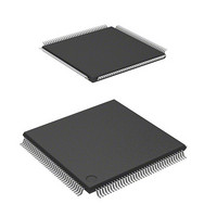
DF2117VT20V Renesas Electronics America, DF2117VT20V Datasheet - Page 807

DF2117VT20V
Manufacturer Part Number
DF2117VT20V
Description
MCU 16BIT FLASH 3V 160K 144-TQFP
Manufacturer
Renesas Electronics America
Series
H8® H8S/2100r
Datasheet
1.DF2117VT20HV.pdf
(1040 pages)
Specifications of DF2117VT20V
Core Processor
H8S/2600
Core Size
16-Bit
Speed
20MHz
Connectivity
FIFO, I²C, LPC, SCI, SmartCard
Peripherals
POR, PWM, WDT
Number Of I /o
112
Program Memory Size
160KB (160K x 8)
Program Memory Type
FLASH
Ram Size
8K x 8
Voltage - Supply (vcc/vdd)
3 V ~ 3.6 V
Data Converters
A/D 16x10b
Oscillator Type
External
Operating Temperature
-20°C ~ 75°C
Package / Case
144-TQFP, 144-VQFP
Lead Free Status / RoHS Status
Lead free / RoHS Compliant
Eeprom Size
-
Available stocks
Company
Part Number
Manufacturer
Quantity
Price
Company:
Part Number:
DF2117VT20V
Manufacturer:
Renesas
Quantity:
100
Company:
Part Number:
DF2117VT20V
Manufacturer:
Renesas Electronics America
Quantity:
10 000
- Current page: 807 of 1040
- Download datasheet (7Mb)
24.7.2
The programming/erasing interface parameters specify the operating frequency, storage place for
program data, start address of programming destination, and erase block number, and exchanges
the execution result. These parameters use the general registers of the CPU (ER0 and ER1) or the
on-chip RAM area. The initial values of programming/erasing interface parameters are undefined
at a power-on reset or a transition to software standby mode.
Since registers of the CPU except for R0L are saved in the stack area during download of an on-
chip program, initialization, programming, or erasing, allocate the stack area before performing
these operations (the maximum stack size is 128 bytes). The return value of the processing result
is written in R0L. The programming/erasing interface parameters are used in download control,
initialization before programming or erasing, programming, and erasing. Table 24.6 shows the
usable parameters and target modes. The meaning of the bits in the flash pass and fail result
parameter (FPFR) varies in initialization, programming, and erasure.
Table 24.6 Parameters and Target Modes
Note:
(a)
The on-chip program is automatically downloaded by setting the SCO bit in FCCS to 1. The on-
chip RAM area to download the on-chip program is the 4-kbyte area starting from the start address
specified by FTDAR. Download is set by the programming/erasing interface registers, and the
download pass and fail result parameter (DPFR) indicates the return value.
Parameter
DPFR
FPFR
FPEFEQ
FMPAR
FMPDR
FEBS
Download Control
* A single byte of the start address of the on-chip RAM specified by FTDAR
Programming/Erasing Interface Parameters
Download
O
⎯
⎯
⎯
⎯
⎯
Initialization
⎯
O
O
⎯
⎯
⎯
Programming
⎯
O
⎯
O
O
⎯
Erasure
⎯
O
⎯
⎯
⎯
O
Rev. 2.00 Sep. 28, 2009 Page 765 of 994
R/W
R/W
R/W
R/W
R/W
R/W
R/W
Initial
Value
Undefined
Undefined
Undefined
Undefined
Undefined
Undefined
REJ09B0452-0200
Allocation
On-chip RAM*
R0L of CPU
ER0 of CPU
ER1 of CPU
ER0 of CPU
ER0 of CPU
Related parts for DF2117VT20V
Image
Part Number
Description
Manufacturer
Datasheet
Request
R

Part Number:
Description:
0.6mm Pitch Board-to-Fine-Coaxial Cable Connectors
Manufacturer:
Hirose Electric
Datasheet:

Part Number:
Description:
0.6mm Pitch Board-to-fine-coaxial Cable Connectors
Manufacturer:
Hirose Electric
Datasheet:

Part Number:
Description:
0.6mm Pitch Board-to-fine-coaxial Cable Connectors
Manufacturer:
Hirose Electric
Datasheet:

Part Number:
Description:
Right angle, Two-piece for fine coaxial cable, Discrete wire connectors; HRS No: 687-0001-5 56; No. of Positions: 20; Connector Type: Board mounting; Contact Gender: Female; Contact Spacing (mm): 0.6; Terminal Pitch (mm): 0.6; PCB Mount Type: SMT; Cu
Manufacturer:
Hirose Electric

Part Number:
Description:
0.6mm Pitch Board-to-fine-coaxial Cable Connectors
Manufacturer:
Hirose Electric
Datasheet:

Part Number:
Description:
0.6mm Pitch Board-to-Fine-Coaxial Cable Connectors
Manufacturer:
HIROSE [Hirose Electric]
Datasheet:

Part Number:
Description:
KIT STARTER FOR M16C/29
Manufacturer:
Renesas Electronics America
Datasheet:

Part Number:
Description:
KIT STARTER FOR R8C/2D
Manufacturer:
Renesas Electronics America
Datasheet:

Part Number:
Description:
R0K33062P STARTER KIT
Manufacturer:
Renesas Electronics America
Datasheet:

Part Number:
Description:
KIT STARTER FOR R8C/23 E8A
Manufacturer:
Renesas Electronics America
Datasheet:

Part Number:
Description:
KIT STARTER FOR R8C/25
Manufacturer:
Renesas Electronics America
Datasheet:

Part Number:
Description:
KIT STARTER H8S2456 SHARPE DSPLY
Manufacturer:
Renesas Electronics America
Datasheet:

Part Number:
Description:
KIT STARTER FOR R8C38C
Manufacturer:
Renesas Electronics America
Datasheet:

Part Number:
Description:
KIT STARTER FOR R8C35C
Manufacturer:
Renesas Electronics America
Datasheet:

Part Number:
Description:
KIT STARTER FOR R8CL3AC+LCD APPS
Manufacturer:
Renesas Electronics America
Datasheet:


