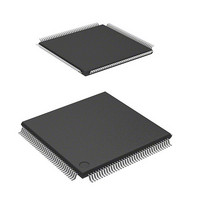
DF2117VT20V Renesas Electronics America, DF2117VT20V Datasheet - Page 677

DF2117VT20V
Manufacturer Part Number
DF2117VT20V
Description
MCU 16BIT FLASH 3V 160K 144-TQFP
Manufacturer
Renesas Electronics America
Series
H8® H8S/2100r
Datasheet
1.DF2117VT20HV.pdf
(1040 pages)
Specifications of DF2117VT20V
Core Processor
H8S/2600
Core Size
16-Bit
Speed
20MHz
Connectivity
FIFO, I²C, LPC, SCI, SmartCard
Peripherals
POR, PWM, WDT
Number Of I /o
112
Program Memory Size
160KB (160K x 8)
Program Memory Type
FLASH
Ram Size
8K x 8
Voltage - Supply (vcc/vdd)
3 V ~ 3.6 V
Data Converters
A/D 16x10b
Oscillator Type
External
Operating Temperature
-20°C ~ 75°C
Package / Case
144-TQFP, 144-VQFP
Lead Free Status / RoHS Status
Lead free / RoHS Compliant
Eeprom Size
-
Available stocks
Company
Part Number
Manufacturer
Quantity
Price
Company:
Part Number:
DF2117VT20V
Manufacturer:
Renesas
Quantity:
100
Company:
Part Number:
DF2117VT20V
Manufacturer:
Renesas Electronics America
Quantity:
10 000
- Current page: 677 of 1040
- Download datasheet (7Mb)
When LPC3E = 1, an I/O address received in an LPC I/O cycle is compared with the contents of
LADR3. When determining an IDR3, ODR3, or STR3 address match, bit 0 in LADR3 is regarded
as 0, and the value of bit 2 is ignored. When determining a TWR0 to TWR15 address match, bit 4
in LADR3 is inverted, and the values of bits 3 to 0 are ignored.
• Host select register
Note:
Bit 4
Bit 4
Bit 4
Bit 4
Bit 4
Bit 4
Bit 4
Bit 4
Bit 4
* When channel 3 is used, the content of LADR3 must be set so that the addresses for
Bit 3
Bit 3
Bit 3
Bit 3
Bit 3
0
0
:
1
0
0
:
1
channels 1, 2, 4, and SCIF are different.
I/O Address
Bit 2
1
0
0
:
1
0
0
:
1
0
1
0
Bit 1
Bit 1
Bit 1
Bit 1
Bit 1
0
0
:
1
0
0
:
1
Bit 0
0
0
0
0
0
1
:
1
0
1
:
1
Transfer
Cycle
I/O write
I/O write
I/O read
I/O read
I/O write
I/O write
I/O read
I/O read
Rev. 2.00 Sep. 28, 2009 Page 635 of 994
Host Select Register
IDR3 write, C/D3 ← 0
IDR3 write, C/D3 ← 1
ODR3 read
STR3 read
TWR0MW write
TWR1 to TWR15 write
TWR0SW read
TWR1 to TWR15 read
REJ09B0452-0200
Related parts for DF2117VT20V
Image
Part Number
Description
Manufacturer
Datasheet
Request
R

Part Number:
Description:
0.6mm Pitch Board-to-Fine-Coaxial Cable Connectors
Manufacturer:
Hirose Electric
Datasheet:

Part Number:
Description:
0.6mm Pitch Board-to-fine-coaxial Cable Connectors
Manufacturer:
Hirose Electric
Datasheet:

Part Number:
Description:
0.6mm Pitch Board-to-fine-coaxial Cable Connectors
Manufacturer:
Hirose Electric
Datasheet:

Part Number:
Description:
Right angle, Two-piece for fine coaxial cable, Discrete wire connectors; HRS No: 687-0001-5 56; No. of Positions: 20; Connector Type: Board mounting; Contact Gender: Female; Contact Spacing (mm): 0.6; Terminal Pitch (mm): 0.6; PCB Mount Type: SMT; Cu
Manufacturer:
Hirose Electric

Part Number:
Description:
0.6mm Pitch Board-to-fine-coaxial Cable Connectors
Manufacturer:
Hirose Electric
Datasheet:

Part Number:
Description:
0.6mm Pitch Board-to-Fine-Coaxial Cable Connectors
Manufacturer:
HIROSE [Hirose Electric]
Datasheet:

Part Number:
Description:
KIT STARTER FOR M16C/29
Manufacturer:
Renesas Electronics America
Datasheet:

Part Number:
Description:
KIT STARTER FOR R8C/2D
Manufacturer:
Renesas Electronics America
Datasheet:

Part Number:
Description:
R0K33062P STARTER KIT
Manufacturer:
Renesas Electronics America
Datasheet:

Part Number:
Description:
KIT STARTER FOR R8C/23 E8A
Manufacturer:
Renesas Electronics America
Datasheet:

Part Number:
Description:
KIT STARTER FOR R8C/25
Manufacturer:
Renesas Electronics America
Datasheet:

Part Number:
Description:
KIT STARTER H8S2456 SHARPE DSPLY
Manufacturer:
Renesas Electronics America
Datasheet:

Part Number:
Description:
KIT STARTER FOR R8C38C
Manufacturer:
Renesas Electronics America
Datasheet:

Part Number:
Description:
KIT STARTER FOR R8C35C
Manufacturer:
Renesas Electronics America
Datasheet:

Part Number:
Description:
KIT STARTER FOR R8CL3AC+LCD APPS
Manufacturer:
Renesas Electronics America
Datasheet:


