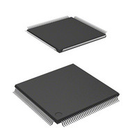
DF2117VT20V Renesas Electronics America, DF2117VT20V Datasheet - Page 201

DF2117VT20V
Manufacturer Part Number
DF2117VT20V
Description
MCU 16BIT FLASH 3V 160K 144-TQFP
Manufacturer
Renesas Electronics America
Series
H8® H8S/2100r
Datasheet
1.DF2117VT20HV.pdf
(1040 pages)
Specifications of DF2117VT20V
Core Processor
H8S/2600
Core Size
16-Bit
Speed
20MHz
Connectivity
FIFO, I²C, LPC, SCI, SmartCard
Peripherals
POR, PWM, WDT
Number Of I /o
112
Program Memory Size
160KB (160K x 8)
Program Memory Type
FLASH
Ram Size
8K x 8
Voltage - Supply (vcc/vdd)
3 V ~ 3.6 V
Data Converters
A/D 16x10b
Oscillator Type
External
Operating Temperature
-20°C ~ 75°C
Package / Case
144-TQFP, 144-VQFP
Lead Free Status / RoHS Status
Lead free / RoHS Compliant
Eeprom Size
-
Available stocks
Company
Part Number
Manufacturer
Quantity
Price
Company:
Part Number:
DF2117VT20V
Manufacturer:
Renesas
Quantity:
100
Company:
Part Number:
DF2117VT20V
Manufacturer:
Renesas Electronics America
Quantity:
10 000
- Current page: 201 of 1040
- Download datasheet (7Mb)
(8)
The pin function is switched as shown below according to the combination of the TMR and the
SCI and the P40DDR bit.
Module
Name
SCI
I/O port
7.2.5
(1)
The pin function is switched as shown below according to the combination of the IIC0AS and
IIC0BS bits in PTCNT1, ICE bit in ICCR of IIC_0, and the P52DDR bit.
Module
Name
IIC
I/O port
Note: To use this pin as SCL0, clear the IIC0AS and IIC0BS bits in PTCNT1 to 0. The output
P40/TMI0/TxD2/TCMCYI0
P52/SCL0
format for SCL0 is NMOS output only and direct bus drive is possible. When this pin is used
as the P52 output pin, the output format is NMOS push-pull.
Port 5
Pin Function
SCL0 output
P52 output
P52 input
(initial setting)
Pin Function
TxD2 output
P40 output
P40 input
(initial setting)
IIC_0
SCL0_OE
1
0
0
SCI
TxD2_OE
1
0
0
Rev. 2.00 Sep. 28, 2009 Page 159 of 994
Setting
Setting
I/O Port
P40DDR
⎯
1
0
I/O Port
P52DDR
⎯
1
0
REJ09B0452-0200
Related parts for DF2117VT20V
Image
Part Number
Description
Manufacturer
Datasheet
Request
R

Part Number:
Description:
0.6mm Pitch Board-to-Fine-Coaxial Cable Connectors
Manufacturer:
Hirose Electric
Datasheet:

Part Number:
Description:
0.6mm Pitch Board-to-fine-coaxial Cable Connectors
Manufacturer:
Hirose Electric
Datasheet:

Part Number:
Description:
0.6mm Pitch Board-to-fine-coaxial Cable Connectors
Manufacturer:
Hirose Electric
Datasheet:

Part Number:
Description:
Right angle, Two-piece for fine coaxial cable, Discrete wire connectors; HRS No: 687-0001-5 56; No. of Positions: 20; Connector Type: Board mounting; Contact Gender: Female; Contact Spacing (mm): 0.6; Terminal Pitch (mm): 0.6; PCB Mount Type: SMT; Cu
Manufacturer:
Hirose Electric

Part Number:
Description:
0.6mm Pitch Board-to-fine-coaxial Cable Connectors
Manufacturer:
Hirose Electric
Datasheet:

Part Number:
Description:
0.6mm Pitch Board-to-Fine-Coaxial Cable Connectors
Manufacturer:
HIROSE [Hirose Electric]
Datasheet:

Part Number:
Description:
KIT STARTER FOR M16C/29
Manufacturer:
Renesas Electronics America
Datasheet:

Part Number:
Description:
KIT STARTER FOR R8C/2D
Manufacturer:
Renesas Electronics America
Datasheet:

Part Number:
Description:
R0K33062P STARTER KIT
Manufacturer:
Renesas Electronics America
Datasheet:

Part Number:
Description:
KIT STARTER FOR R8C/23 E8A
Manufacturer:
Renesas Electronics America
Datasheet:

Part Number:
Description:
KIT STARTER FOR R8C/25
Manufacturer:
Renesas Electronics America
Datasheet:

Part Number:
Description:
KIT STARTER H8S2456 SHARPE DSPLY
Manufacturer:
Renesas Electronics America
Datasheet:

Part Number:
Description:
KIT STARTER FOR R8C38C
Manufacturer:
Renesas Electronics America
Datasheet:

Part Number:
Description:
KIT STARTER FOR R8C35C
Manufacturer:
Renesas Electronics America
Datasheet:

Part Number:
Description:
KIT STARTER FOR R8CL3AC+LCD APPS
Manufacturer:
Renesas Electronics America
Datasheet:


