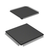
DF2117VT20V Renesas Electronics America, DF2117VT20V Datasheet - Page 217

DF2117VT20V
Manufacturer Part Number
DF2117VT20V
Description
MCU 16BIT FLASH 3V 160K 144-TQFP
Manufacturer
Renesas Electronics America
Series
H8® H8S/2100r
Datasheet
1.DF2117VT20HV.pdf
(1040 pages)
Specifications of DF2117VT20V
Core Processor
H8S/2600
Core Size
16-Bit
Speed
20MHz
Connectivity
FIFO, I²C, LPC, SCI, SmartCard
Peripherals
POR, PWM, WDT
Number Of I /o
112
Program Memory Size
160KB (160K x 8)
Program Memory Type
FLASH
Ram Size
8K x 8
Voltage - Supply (vcc/vdd)
3 V ~ 3.6 V
Data Converters
A/D 16x10b
Oscillator Type
External
Operating Temperature
-20°C ~ 75°C
Package / Case
144-TQFP, 144-VQFP
Lead Free Status / RoHS Status
Lead free / RoHS Compliant
Eeprom Size
-
Available stocks
Company
Part Number
Manufacturer
Quantity
Price
Company:
Part Number:
DF2117VT20V
Manufacturer:
Renesas
Quantity:
100
Company:
Part Number:
DF2117VT20V
Manufacturer:
Renesas Electronics America
Quantity:
10 000
- Current page: 217 of 1040
- Download datasheet (7Mb)
(5)
The pin function is switched as shown below according to the combination of the register setting
of the TPU and the PC3DDR bit. When the WUEMR11 bit in WUEMR of the interrupt controller
is cleared to 0, this pin can be used as the WUE11 input pin.
This pin functions as TCLKB input when TPSC2 to TPSC0 in any of TCR_0 to TCR_2 are set to
B'101 or when channel 1 is set to phase counting mode.
This pin functions as TIOCD1 input when TPU channel 0 timer operating mode is set to normal
operation or phase counting mode and IOD3 to IOD0 in TIOR_0 are set to B'10xx. (x: Don't care.)
Module
Name
TPU
I/O port
(6)
The pin function is switched as shown below according to the combination of the register setting
of the TPU and the PC2DDR bit. When the WUEMR10 bit in WUEMR of the interrupt controller
is cleared to 0, this pin can be used as the WUE10 input pin.
This pin functions as TCLKA input when TPSC2 to TPSC0 in any of TCR_0 to TCR_2 are set to
B'100 or when channel 1 is set to phase counting mode.
This pin functions as TIOCC0 input when TPU channel 0 timer operating mode is set to normal
operation or phase counting mode and IOC3 to IOC0 in TIOR_0 are set to B'10xx. (x: Don't care.)
Module
Name
TPU
I/O port
PC3/WUE11/TIOCD0/TCLKB
PC2/WUE10/TIOCC0/TCLKA
Pin Function
TIOCD0 output
PC3 output
PC3 input
(initial setting)
Pin Function
TIOCC0 output
PC2 output
PC2 input
(initial setting)
TPU
TIOCD0_OE
1
0
0
TPU
TIOCC0_OE
1
0
0
Rev. 2.00 Sep. 28, 2009 Page 175 of 994
Setting
Setting
I/O Port
PC3DDR
⎯
1
0
I/O Port
PC2DDR
⎯
1
0
REJ09B0452-0200
Related parts for DF2117VT20V
Image
Part Number
Description
Manufacturer
Datasheet
Request
R

Part Number:
Description:
0.6mm Pitch Board-to-Fine-Coaxial Cable Connectors
Manufacturer:
Hirose Electric
Datasheet:

Part Number:
Description:
0.6mm Pitch Board-to-fine-coaxial Cable Connectors
Manufacturer:
Hirose Electric
Datasheet:

Part Number:
Description:
0.6mm Pitch Board-to-fine-coaxial Cable Connectors
Manufacturer:
Hirose Electric
Datasheet:

Part Number:
Description:
Right angle, Two-piece for fine coaxial cable, Discrete wire connectors; HRS No: 687-0001-5 56; No. of Positions: 20; Connector Type: Board mounting; Contact Gender: Female; Contact Spacing (mm): 0.6; Terminal Pitch (mm): 0.6; PCB Mount Type: SMT; Cu
Manufacturer:
Hirose Electric

Part Number:
Description:
0.6mm Pitch Board-to-fine-coaxial Cable Connectors
Manufacturer:
Hirose Electric
Datasheet:

Part Number:
Description:
0.6mm Pitch Board-to-Fine-Coaxial Cable Connectors
Manufacturer:
HIROSE [Hirose Electric]
Datasheet:

Part Number:
Description:
KIT STARTER FOR M16C/29
Manufacturer:
Renesas Electronics America
Datasheet:

Part Number:
Description:
KIT STARTER FOR R8C/2D
Manufacturer:
Renesas Electronics America
Datasheet:

Part Number:
Description:
R0K33062P STARTER KIT
Manufacturer:
Renesas Electronics America
Datasheet:

Part Number:
Description:
KIT STARTER FOR R8C/23 E8A
Manufacturer:
Renesas Electronics America
Datasheet:

Part Number:
Description:
KIT STARTER FOR R8C/25
Manufacturer:
Renesas Electronics America
Datasheet:

Part Number:
Description:
KIT STARTER H8S2456 SHARPE DSPLY
Manufacturer:
Renesas Electronics America
Datasheet:

Part Number:
Description:
KIT STARTER FOR R8C38C
Manufacturer:
Renesas Electronics America
Datasheet:

Part Number:
Description:
KIT STARTER FOR R8C35C
Manufacturer:
Renesas Electronics America
Datasheet:

Part Number:
Description:
KIT STARTER FOR R8CL3AC+LCD APPS
Manufacturer:
Renesas Electronics America
Datasheet:


