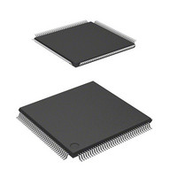
DF2117VT20V Renesas Electronics America, DF2117VT20V Datasheet - Page 745

DF2117VT20V
Manufacturer Part Number
DF2117VT20V
Description
MCU 16BIT FLASH 3V 160K 144-TQFP
Manufacturer
Renesas Electronics America
Series
H8® H8S/2100r
Datasheet
1.DF2117VT20HV.pdf
(1040 pages)
Specifications of DF2117VT20V
Core Processor
H8S/2600
Core Size
16-Bit
Speed
20MHz
Connectivity
FIFO, I²C, LPC, SCI, SmartCard
Peripherals
POR, PWM, WDT
Number Of I /o
112
Program Memory Size
160KB (160K x 8)
Program Memory Type
FLASH
Ram Size
8K x 8
Voltage - Supply (vcc/vdd)
3 V ~ 3.6 V
Data Converters
A/D 16x10b
Oscillator Type
External
Operating Temperature
-20°C ~ 75°C
Package / Case
144-TQFP, 144-VQFP
Lead Free Status / RoHS Status
Lead free / RoHS Compliant
Eeprom Size
-
Available stocks
Company
Part Number
Manufacturer
Quantity
Price
Company:
Part Number:
DF2117VT20V
Manufacturer:
Renesas
Quantity:
100
Company:
Part Number:
DF2117VT20V
Manufacturer:
Renesas Electronics America
Quantity:
10 000
- Current page: 745 of 1040
- Download datasheet (7Mb)
21.4
21.4.1
Table 21.4 LPC Memory Read/Write Cycles
In LPC/FW memory read and write cycles, data is transferred using LAD3 to LAD0
synchronously with LCLK. The order of data transfer is shown in table 21.4. In a cycle returning
synchronization signal from the slave, the slave usually returns B'1010 to notify the host of error
occurrence; while the FSI in this LSI always returns B'0000 (Ready) or B'0110 (Long wait).
The FSI becomes busy if the received address matches an address in the host accessible range set
in the registers (FSIHBARH, FSIHBARL, FSISR, and CMDHBAR), and outputs a turn-around
signal to return to the idle state.
State
Counts Content
1
2
3
4
5
6
7
8
9
10
11
12
13
Start
Cycle type/
direction
Address 1
Address 2
Address 3
Address 4
Address 5
Address 6
Address 7
Address 8
Turn-around
(recovery)
Turn-around None
Wait*
Operation
LPC/FW Memory Cycles
LPC Memory Read Cycles
Driven by
Host
Host
Host
Host
Host
Host
Host
Host
Host
Host
Host
Slave
Value (3 to 0)
0000
0100
bit 31 to bit 28
bit 27 to bit 24
bit 23 to bit 20
bit 19 to bit 16
bit 15 to bit 12
bit 11 to bit 8
bit 7 to bit 4
bit 3 to bit 0
1111
ZZZZ
0110
Content
Start
Cycle type/
direction
Address 1
Address 2
Address 3
Address 4
Address 5
Address 6
Address 7
Address 8
Data 1
Data 2
Turn-around
(recovery)
Rev. 2.00 Sep. 28, 2009 Page 703 of 994
LPC Memory Write Cycles
Host
Host
Host
Host
Host
Host
Host
Host
Host
Host
Host
Driven by
Host
Host
REJ09B0452-0200
0110
bit 31 to bit 28
bit 27 to bit 24
bit 23 to bit 20
bit 19 to bit 16
bit 15 to bit 12
bit 11 to bit 8
bit 7 to bit 4
bit 3 to bit 0
bit 3 to bit 0
bit 7 to bit 4
1111
Value (3 to 0)
0000
Related parts for DF2117VT20V
Image
Part Number
Description
Manufacturer
Datasheet
Request
R

Part Number:
Description:
0.6mm Pitch Board-to-Fine-Coaxial Cable Connectors
Manufacturer:
Hirose Electric
Datasheet:

Part Number:
Description:
0.6mm Pitch Board-to-fine-coaxial Cable Connectors
Manufacturer:
Hirose Electric
Datasheet:

Part Number:
Description:
0.6mm Pitch Board-to-fine-coaxial Cable Connectors
Manufacturer:
Hirose Electric
Datasheet:

Part Number:
Description:
Right angle, Two-piece for fine coaxial cable, Discrete wire connectors; HRS No: 687-0001-5 56; No. of Positions: 20; Connector Type: Board mounting; Contact Gender: Female; Contact Spacing (mm): 0.6; Terminal Pitch (mm): 0.6; PCB Mount Type: SMT; Cu
Manufacturer:
Hirose Electric

Part Number:
Description:
0.6mm Pitch Board-to-fine-coaxial Cable Connectors
Manufacturer:
Hirose Electric
Datasheet:

Part Number:
Description:
0.6mm Pitch Board-to-Fine-Coaxial Cable Connectors
Manufacturer:
HIROSE [Hirose Electric]
Datasheet:

Part Number:
Description:
KIT STARTER FOR M16C/29
Manufacturer:
Renesas Electronics America
Datasheet:

Part Number:
Description:
KIT STARTER FOR R8C/2D
Manufacturer:
Renesas Electronics America
Datasheet:

Part Number:
Description:
R0K33062P STARTER KIT
Manufacturer:
Renesas Electronics America
Datasheet:

Part Number:
Description:
KIT STARTER FOR R8C/23 E8A
Manufacturer:
Renesas Electronics America
Datasheet:

Part Number:
Description:
KIT STARTER FOR R8C/25
Manufacturer:
Renesas Electronics America
Datasheet:

Part Number:
Description:
KIT STARTER H8S2456 SHARPE DSPLY
Manufacturer:
Renesas Electronics America
Datasheet:

Part Number:
Description:
KIT STARTER FOR R8C38C
Manufacturer:
Renesas Electronics America
Datasheet:

Part Number:
Description:
KIT STARTER FOR R8C35C
Manufacturer:
Renesas Electronics America
Datasheet:

Part Number:
Description:
KIT STARTER FOR R8CL3AC+LCD APPS
Manufacturer:
Renesas Electronics America
Datasheet:


