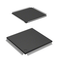
DF2117VT20V Renesas Electronics America, DF2117VT20V Datasheet - Page 749

DF2117VT20V
Manufacturer Part Number
DF2117VT20V
Description
MCU 16BIT FLASH 3V 160K 144-TQFP
Manufacturer
Renesas Electronics America
Series
H8® H8S/2100r
Datasheet
1.DF2117VT20HV.pdf
(1040 pages)
Specifications of DF2117VT20V
Core Processor
H8S/2600
Core Size
16-Bit
Speed
20MHz
Connectivity
FIFO, I²C, LPC, SCI, SmartCard
Peripherals
POR, PWM, WDT
Number Of I /o
112
Program Memory Size
160KB (160K x 8)
Program Memory Type
FLASH
Ram Size
8K x 8
Voltage - Supply (vcc/vdd)
3 V ~ 3.6 V
Data Converters
A/D 16x10b
Oscillator Type
External
Operating Temperature
-20°C ~ 75°C
Package / Case
144-TQFP, 144-VQFP
Lead Free Status / RoHS Status
Lead free / RoHS Compliant
Eeprom Size
-
Available stocks
Company
Part Number
Manufacturer
Quantity
Price
Company:
Part Number:
DF2117VT20V
Manufacturer:
Renesas
Quantity:
100
Company:
Part Number:
DF2117VT20V
Manufacturer:
Renesas Electronics America
Quantity:
10 000
- Current page: 749 of 1040
- Download datasheet (7Mb)
21.4.4
The FSI supports direct transfer between the host and SPI flash memory. If the host address input
in LPC/FW memory write cycle matches the host address set in FSIHBARH, FSIHBARL, or
FSISR, the FSI memory cycle starts. In LPC/FW memory write cycle, the FSI supports three types
of instructions: Byte/Page-Program instructions and AAI-Program instruction. In LPC/FW
memory read cycle, the FSI supports two types of instructions: Read instruction and Fast-Read
instruction. In the case that LPC-SPI direct transfer is selected in Byte-Program, Page-Program, or
AAI-Program instruction execution, set FLDCT of SLCR to 1. The FSI reads the data with LPC-
SPI direct transfer regardless of the status of FLDCT in Read and Fast-Read instruction execution.
(1)
The host address can be converted into the SPI flash memory address by setting FSIHBARH,
FSIHBARL, and FSISR. The host address space ranges from H'0000_0000 to H'FFFF_FFFF. The
SPI flash memory address space ranges from H'00_0000 to H'FF_FFFF. Figure 21.3 shows an
example of the FSI memory address conversion.
As shown in figure 21.3, if an address ranging from H'231F_0000 to H'232E_FFFF is accessed in
LPC/FW memory write cycle, the SPI flash memory is accessed. If a host address to be input is
out of the determined range, Sync will not be returned. During an SPI flash memory access, a long
wait cycle will be inserted to the LPC bus cycle. In an LPC memory cycle, one-byte transfer is
enabled. In an FW memory cycle, a byte, word, and a longword transfer are enabled.
FSIHBAR: H'231F
FSISR: H'00 (1 MB)
Note: * The upper 16 bits of the host address are set to the value in the FSIHBAR register.
FSI Address Conversion
FSI Memory Cycle (Direct Transfer between LPC and SPI)
H'231F_0000 *
H'232E_FFFF
Figure 21.3 FSI Address Conversion Example
Host addresses
1MB
1 MB
Rev. 2.00 Sep. 28, 2009 Page 707 of 994
SPI flash memory
SPI addresses
1 MB
REJ09B0452-0200
H'00_0000
H'0F_FFFF
Related parts for DF2117VT20V
Image
Part Number
Description
Manufacturer
Datasheet
Request
R

Part Number:
Description:
0.6mm Pitch Board-to-Fine-Coaxial Cable Connectors
Manufacturer:
Hirose Electric
Datasheet:

Part Number:
Description:
0.6mm Pitch Board-to-fine-coaxial Cable Connectors
Manufacturer:
Hirose Electric
Datasheet:

Part Number:
Description:
0.6mm Pitch Board-to-fine-coaxial Cable Connectors
Manufacturer:
Hirose Electric
Datasheet:

Part Number:
Description:
Right angle, Two-piece for fine coaxial cable, Discrete wire connectors; HRS No: 687-0001-5 56; No. of Positions: 20; Connector Type: Board mounting; Contact Gender: Female; Contact Spacing (mm): 0.6; Terminal Pitch (mm): 0.6; PCB Mount Type: SMT; Cu
Manufacturer:
Hirose Electric

Part Number:
Description:
0.6mm Pitch Board-to-fine-coaxial Cable Connectors
Manufacturer:
Hirose Electric
Datasheet:

Part Number:
Description:
0.6mm Pitch Board-to-Fine-Coaxial Cable Connectors
Manufacturer:
HIROSE [Hirose Electric]
Datasheet:

Part Number:
Description:
KIT STARTER FOR M16C/29
Manufacturer:
Renesas Electronics America
Datasheet:

Part Number:
Description:
KIT STARTER FOR R8C/2D
Manufacturer:
Renesas Electronics America
Datasheet:

Part Number:
Description:
R0K33062P STARTER KIT
Manufacturer:
Renesas Electronics America
Datasheet:

Part Number:
Description:
KIT STARTER FOR R8C/23 E8A
Manufacturer:
Renesas Electronics America
Datasheet:

Part Number:
Description:
KIT STARTER FOR R8C/25
Manufacturer:
Renesas Electronics America
Datasheet:

Part Number:
Description:
KIT STARTER H8S2456 SHARPE DSPLY
Manufacturer:
Renesas Electronics America
Datasheet:

Part Number:
Description:
KIT STARTER FOR R8C38C
Manufacturer:
Renesas Electronics America
Datasheet:

Part Number:
Description:
KIT STARTER FOR R8C35C
Manufacturer:
Renesas Electronics America
Datasheet:

Part Number:
Description:
KIT STARTER FOR R8CL3AC+LCD APPS
Manufacturer:
Renesas Electronics America
Datasheet:


