HD64F2239TF20I Renesas Electronics America, HD64F2239TF20I Datasheet - Page 16
HD64F2239TF20I
Manufacturer Part Number
HD64F2239TF20I
Description
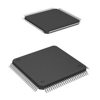
MCU 3V 384K I-TEMP 100-TQFP
Manufacturer
Renesas Electronics America
Series
H8® H8S/2200r
Datasheet
1.DF2238RFA6V.pdf
(1048 pages)
Specifications of HD64F2239TF20I
Core Processor
H8S/2000
Core Size
16-Bit
Speed
20MHz
Connectivity
I²C, SCI, SmartCard
Peripherals
DMA, POR, PWM, WDT
Number Of I /o
72
Program Memory Size
384KB (384K x 8)
Program Memory Type
FLASH
Ram Size
32K x 8
Voltage - Supply (vcc/vdd)
2.7 V ~ 3.6 V
Data Converters
A/D 8x10b; D/A 2x8b
Oscillator Type
Internal
Operating Temperature
-40°C ~ 85°C
Package / Case
100-TQFP, 100-VQFP
Lead Free Status / RoHS Status
Contains lead / RoHS non-compliant
Eeprom Size
-
Available stocks
Company
Part Number
Manufacturer
Quantity
Price
Company:

Part Number:
HD64F2239TF20I
Manufacturer:
Renesas Electronics America
Quantity:
10 000


Item
11.3.1 Timer Control
Register (TCR)
13.3.1 Timer Counter
(TCNT)
13.6.3 Changing Value of
PSS or CKS2 to CKS0
13.6.7 Notes on Initializing
TCNT by Using the TME Bit
15.3.8 Smart Card Mode
Register (SCMR)
Rev. 6.00 Mar. 18, 2010 Page xiv of lx
REJ09B0054-0600
Page
367
468
479
479
570
Revision (See Manual for Details)
Table amended
Description added
TCNT is an 8-bit readable/writable up-counter. TCNT is
initialized to H'00 when the TME bit in TCSR is cleared to 0.
To initialize TCNT to H'00 while the timer is operating, write
H'00 to TCNT directly. See 13.6.7, Notes on Initializing
TCNT by Using the TME Bit.
Description amended
If the PSS or CKS0 to CKS2 bits in TCSR are written to
while the WDT is operating, errors could occur in the
incrementation. Software must be used to stop the watchdog
timer (by clearing the TME bit to 0) before changing the
value of the PSS or CKS0 to CKS2 bits.
13.6.7 added
Table amended
Bit
4
3
Bit
7 to 4
3
Bit Name
CKEG1
CKEG0
Bit Name
—
SDIR
Initial Value
0
0
Initial
Value
All 1
0
R/W
R/W
R/W
R/W
—
R/W
Description
Clock Edge 1 and 0
These bits select the input clock edge. When the input
clock is counted using both edges, the input clock
period is halved (e.g. φ/4 both edges = φ/2 rising
edge). If phase counting mode is used on channels 1,
2, 4 * , and 5 * , this setting is ignored and the phase
counting mode setting has priority. Internal clock edge
selection is valid when the input clock is /4 or slower.
When the input clock is φ/1 or when
overflow/underflow of another channel is selected,
this setting is ignored and the input clock is counted at
the falling edge of φ.
00: Count at rising edge
01: Count at falling edge
1 : Count at both edges
Legend:
Description
Reserved
These bits are always read as 1, and cannot be
modified.
Smart Card Data Transfer Direction
Selects the serial/parallel conversion format.
0: LSB-first in transfer
1: MSB-first in transfer
The bit setting is valid only when the transfer data
format is 8 bits. Except in the case of 7-bit data in
asynchronous mode, either LSB-first or MSB-first
may be selected regardless of the serial
communication mode. For 7-bit data, set this bit to
0 to select LSB-first in transfer.
×
: Don’t care
Related parts for HD64F2239TF20I
Image
Part Number
Description
Manufacturer
Datasheet
Request
R

Part Number:
Description:
KIT STARTER FOR M16C/29
Manufacturer:
Renesas Electronics America
Datasheet:

Part Number:
Description:
KIT STARTER FOR R8C/2D
Manufacturer:
Renesas Electronics America
Datasheet:

Part Number:
Description:
R0K33062P STARTER KIT
Manufacturer:
Renesas Electronics America
Datasheet:

Part Number:
Description:
KIT STARTER FOR R8C/23 E8A
Manufacturer:
Renesas Electronics America
Datasheet:

Part Number:
Description:
KIT STARTER FOR R8C/25
Manufacturer:
Renesas Electronics America
Datasheet:

Part Number:
Description:
KIT STARTER H8S2456 SHARPE DSPLY
Manufacturer:
Renesas Electronics America
Datasheet:

Part Number:
Description:
KIT STARTER FOR R8C38C
Manufacturer:
Renesas Electronics America
Datasheet:

Part Number:
Description:
KIT STARTER FOR R8C35C
Manufacturer:
Renesas Electronics America
Datasheet:

Part Number:
Description:
KIT STARTER FOR R8CL3AC+LCD APPS
Manufacturer:
Renesas Electronics America
Datasheet:
Part Number:
Description:
KIT STARTER FOR RX610
Manufacturer:
Renesas Electronics America
Datasheet:

Part Number:
Description:
KIT STARTER FOR R32C/118
Manufacturer:
Renesas Electronics America
Datasheet:

Part Number:
Description:
KIT DEV RSK-R8C/26-29
Manufacturer:
Renesas Electronics America
Datasheet:

Part Number:
Description:
KIT STARTER FOR SH7124
Manufacturer:
Renesas Electronics America
Datasheet:

Part Number:
Description:
KIT STARTER FOR H8SX/1622
Manufacturer:
Renesas Electronics America
Datasheet:

Part Number:
Description:
KIT DEV FOR SH7203
Manufacturer:
Renesas Electronics America
Datasheet: