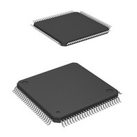
HD64F2239TF20I Renesas Electronics America, HD64F2239TF20I Datasheet - Page 51

HD64F2239TF20I
Manufacturer Part Number
HD64F2239TF20I
Description
MCU 3V 384K I-TEMP 100-TQFP
Manufacturer
Renesas Electronics America
Series
H8® H8S/2200r
Datasheet
1.DF2238RFA6V.pdf
(1048 pages)
Specifications of HD64F2239TF20I
Core Processor
H8S/2000
Core Size
16-Bit
Speed
20MHz
Connectivity
I²C, SCI, SmartCard
Peripherals
DMA, POR, PWM, WDT
Number Of I /o
72
Program Memory Size
384KB (384K x 8)
Program Memory Type
FLASH
Ram Size
32K x 8
Voltage - Supply (vcc/vdd)
2.7 V ~ 3.6 V
Data Converters
A/D 8x10b; D/A 2x8b
Oscillator Type
Internal
Operating Temperature
-40°C ~ 85°C
Package / Case
100-TQFP, 100-VQFP
Lead Free Status / RoHS Status
Contains lead / RoHS non-compliant
Eeprom Size
-
Available stocks
Company
Part Number
Manufacturer
Quantity
Price
Company:
Part Number:
HD64F2239TF20I
Manufacturer:
Renesas Electronics America
Quantity:
10 000
- Current page: 51 of 1048
- Download datasheet (6Mb)
Section 17 A/D Converter
Figure 17.1
Figure 17.2
Figure 17.3
Figure 17.4
Figure 17.5
Figure 17.6
Figure 17.7
Figure 17.8
Figure 17.9
Figure 17.10 Example of Analog Input Protection Circuit........................................................706
Figure 17.11 Analog Input Pin Equivalent Circuit ....................................................................706
Section 18 D/A Converter
Figure 18.1
Figure 18.2
Section 20 Flash Memory (F-ZTAT Version)
Figure 20.1
Figure 20.2
Figure 20.3
Figure 20.4
Figure 20.5
Figure 20.6
Figure 20.7
Figure 20.8
Figure 20.9
Figure 20.10 Example of RAM Overlap Operation...................................................................737
Figure 20.11 Program/Program-Verify Flowchart ....................................................................739
Figure 20.12 Erase/Erase-Verify Flowchart ..............................................................................741
Figure 20.13 Socket Adapter Pin Correspondence Diagram .....................................................744
Figure 20.14 Power-On/Off Timing (Boot Mode) ....................................................................748
Figure 20.15 Power-On/Off Timing (User Program Mode)......................................................749
Figure 20.16 Mode Transition Timing
Section 21 Masked ROM
Figure 21.1
Block Diagram of A/D Converter ........................................................................690
Access to ADDR (When Reading H'AA40) ........................................................696
Example of A/D converter Operation (Single Mode, Channel 1 Selected)..........698
Example of A/D Converter Operation
(Scan Mode, Channels AN0 to AN2 Selected) ....................................................699
A/D Conversion Timing.......................................................................................700
External Trigger Input Timing .............................................................................701
A/D Conversion Accuracy Definitions ................................................................703
A/D Conversion Accuracy Definitions ................................................................703
Example of Analog Input Circuit .........................................................................704
Block Diagram of D/A Converter ........................................................................707
D/A Converter Operation Example......................................................................710
Block Diagram of Flash Memory.........................................................................716
Flash Memory State Transitions...........................................................................717
Boot Mode (Example)..........................................................................................718
User Program Mode (Example) ...........................................................................719
Block Configuration of 384-kbyte Flash Memory ...............................................721
Block Configuration of 256-kbyte Flash Memory ...............................................722
Block Configuration of 128-kbyte Flash Memory ...............................................723
Programming/Erasing Flowchart Example in User Program Mode.....................735
Flowchart for Flash Memory Emulation in RAM ................................................736
(Example: Boot Mode → User Mode ↔ User Program Mode)...........................750
Block Diagram of On-Chip Masked ROM (384 kbytes).....................................754
Rev. 6.00 Mar. 18, 2010 Page xlix of lx
REJ09B0054-0600
Related parts for HD64F2239TF20I
Image
Part Number
Description
Manufacturer
Datasheet
Request
R

Part Number:
Description:
KIT STARTER FOR M16C/29
Manufacturer:
Renesas Electronics America
Datasheet:

Part Number:
Description:
KIT STARTER FOR R8C/2D
Manufacturer:
Renesas Electronics America
Datasheet:

Part Number:
Description:
R0K33062P STARTER KIT
Manufacturer:
Renesas Electronics America
Datasheet:

Part Number:
Description:
KIT STARTER FOR R8C/23 E8A
Manufacturer:
Renesas Electronics America
Datasheet:

Part Number:
Description:
KIT STARTER FOR R8C/25
Manufacturer:
Renesas Electronics America
Datasheet:

Part Number:
Description:
KIT STARTER H8S2456 SHARPE DSPLY
Manufacturer:
Renesas Electronics America
Datasheet:

Part Number:
Description:
KIT STARTER FOR R8C38C
Manufacturer:
Renesas Electronics America
Datasheet:

Part Number:
Description:
KIT STARTER FOR R8C35C
Manufacturer:
Renesas Electronics America
Datasheet:

Part Number:
Description:
KIT STARTER FOR R8CL3AC+LCD APPS
Manufacturer:
Renesas Electronics America
Datasheet:

Part Number:
Description:
KIT STARTER FOR RX610
Manufacturer:
Renesas Electronics America
Datasheet:

Part Number:
Description:
KIT STARTER FOR R32C/118
Manufacturer:
Renesas Electronics America
Datasheet:

Part Number:
Description:
KIT DEV RSK-R8C/26-29
Manufacturer:
Renesas Electronics America
Datasheet:

Part Number:
Description:
KIT STARTER FOR SH7124
Manufacturer:
Renesas Electronics America
Datasheet:

Part Number:
Description:
KIT STARTER FOR H8SX/1622
Manufacturer:
Renesas Electronics America
Datasheet:

Part Number:
Description:
KIT DEV FOR SH7203
Manufacturer:
Renesas Electronics America
Datasheet:


