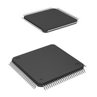
HD64F2239TF20I Renesas Electronics America, HD64F2239TF20I Datasheet - Page 45

HD64F2239TF20I
Manufacturer Part Number
HD64F2239TF20I
Description
MCU 3V 384K I-TEMP 100-TQFP
Manufacturer
Renesas Electronics America
Series
H8® H8S/2200r
Datasheet
1.DF2238RFA6V.pdf
(1048 pages)
Specifications of HD64F2239TF20I
Core Processor
H8S/2000
Core Size
16-Bit
Speed
20MHz
Connectivity
I²C, SCI, SmartCard
Peripherals
DMA, POR, PWM, WDT
Number Of I /o
72
Program Memory Size
384KB (384K x 8)
Program Memory Type
FLASH
Ram Size
32K x 8
Voltage - Supply (vcc/vdd)
2.7 V ~ 3.6 V
Data Converters
A/D 8x10b; D/A 2x8b
Oscillator Type
Internal
Operating Temperature
-40°C ~ 85°C
Package / Case
100-TQFP, 100-VQFP
Lead Free Status / RoHS Status
Contains lead / RoHS non-compliant
Eeprom Size
-
Available stocks
Company
Part Number
Manufacturer
Quantity
Price
Company:
Part Number:
HD64F2239TF20I
Manufacturer:
Renesas Electronics America
Quantity:
10 000
- Current page: 45 of 1048
- Download datasheet (6Mb)
Figure 8.15
Figure 8.16
Figure 8.17
Figure 8.18
Figure 8.19
Figure 8.20
Figure 8.21
Figure 8.22
Figure 8.23
Figure 8.24
Figure 8.25
Figure 8.26
Figure 8.27
Figure 8.28
Figure 8.29
Figure 8.30
Figure 8.31
Figure 8.32
Figure 8.33
Figure 8.34
Figure 8.35
Figure 8.36
Figure 8.37
Figure 8.38
Figure 8.39
Section 9 Data Transfer Controller (DTC)
Figure 9.1
Figure 9.2
Figure 9.3
Figure 9.4
Figure 9.5
Figure 9.6
Figure 9.7
Figure 9.8
Figure 9.9
Figure 9.10
Figure 9.11
Operation in Block Transfer Mode (BLKDIR = 1)..............................................253
Operation Flow in Block Transfer Mode .............................................................254
Example of Block Transfer Mode Setting Procedure...........................................255
Example of DMA Transfer Bus Timing...............................................................256
Example of Short Address Mode Transfer...........................................................257
Example of Full Address Mode Transfer (Cycle Steal) .......................................258
Example of Full Address Mode Transfer (Burst Mode).......................................259
Example of Full Address Mode Transfer (Block Transfer Mode) .......................260
Example of DREQ Pin Falling Edge Activated Normal Mode Transfer .............261
Example of DREQ Pin Falling Edge Activated Block Transfer Mode Transfer..262
Example of DREQ Pin Low Level Activated Normal Mode Transfer.................263
Example of DREQ Pin Low Level Activated Block Transfer Mode Transfer.....264
Example of Single Address Mode Transfer (Byte Read) .....................................265
Example of Single Address Mode (Word Read) Transfer....................................266
Example of Single Address Mode Transfer (Byte Write) ....................................267
Example of Single Address Mode Transfer (Word Write)...................................268
Example of DREQ Pin Falling Edge Activated Single Address Mode Transfer .269
Example of DREQ Pin Low Level Activated Single Address Mode Transfer.....270
Example of Multi-Channel Transfer ....................................................................272
Example of Procedure for Continuing Transfer on Channel Interrupted by NMI
Interrupt................................................................................................................273
Example of Procedure for Forcibly Terminating DMAC Operation....................274
Example of Procedure for Clearing Full Address Mode ......................................274
Block Diagram of Transfer End/Transfer Break Interrupt ...................................275
DMAC Register Update Timing ..........................................................................276
Contention between DMAC Register Update and CPU Read..............................277
Block Diagram of DTC ........................................................................................282
Block Diagram of DTC Activation Source Control .............................................289
The Location of the DTC Register Information in the Address Space.................290
Correspondence between DTC Vector Address and Register Information ..........290
Flowchart of DTC Operation ...............................................................................293
Memory Mapping in Normal Mode .....................................................................294
Memory Mapping in Repeat Mode ......................................................................295
Memory Mapping in Block Transfer Mode .........................................................296
Chain Transfer Operation.....................................................................................297
DTC Operation Timing (Example in Normal Mode or Repeat Mode) ................298
DTC Operation Timing (Example of Block Transfer Mode, with Block
Size of 2) ..............................................................................................................299
Rev. 6.00 Mar. 18, 2010 Page xliii of lx
REJ09B0054-0600
Related parts for HD64F2239TF20I
Image
Part Number
Description
Manufacturer
Datasheet
Request
R

Part Number:
Description:
KIT STARTER FOR M16C/29
Manufacturer:
Renesas Electronics America
Datasheet:

Part Number:
Description:
KIT STARTER FOR R8C/2D
Manufacturer:
Renesas Electronics America
Datasheet:

Part Number:
Description:
R0K33062P STARTER KIT
Manufacturer:
Renesas Electronics America
Datasheet:

Part Number:
Description:
KIT STARTER FOR R8C/23 E8A
Manufacturer:
Renesas Electronics America
Datasheet:

Part Number:
Description:
KIT STARTER FOR R8C/25
Manufacturer:
Renesas Electronics America
Datasheet:

Part Number:
Description:
KIT STARTER H8S2456 SHARPE DSPLY
Manufacturer:
Renesas Electronics America
Datasheet:

Part Number:
Description:
KIT STARTER FOR R8C38C
Manufacturer:
Renesas Electronics America
Datasheet:

Part Number:
Description:
KIT STARTER FOR R8C35C
Manufacturer:
Renesas Electronics America
Datasheet:

Part Number:
Description:
KIT STARTER FOR R8CL3AC+LCD APPS
Manufacturer:
Renesas Electronics America
Datasheet:

Part Number:
Description:
KIT STARTER FOR RX610
Manufacturer:
Renesas Electronics America
Datasheet:

Part Number:
Description:
KIT STARTER FOR R32C/118
Manufacturer:
Renesas Electronics America
Datasheet:

Part Number:
Description:
KIT DEV RSK-R8C/26-29
Manufacturer:
Renesas Electronics America
Datasheet:

Part Number:
Description:
KIT STARTER FOR SH7124
Manufacturer:
Renesas Electronics America
Datasheet:

Part Number:
Description:
KIT STARTER FOR H8SX/1622
Manufacturer:
Renesas Electronics America
Datasheet:

Part Number:
Description:
KIT DEV FOR SH7203
Manufacturer:
Renesas Electronics America
Datasheet:


