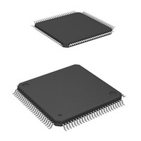
HD64F2239TF20I Renesas Electronics America, HD64F2239TF20I Datasheet - Page 48

HD64F2239TF20I
Manufacturer Part Number
HD64F2239TF20I
Description
MCU 3V 384K I-TEMP 100-TQFP
Manufacturer
Renesas Electronics America
Series
H8® H8S/2200r
Datasheet
1.DF2238RFA6V.pdf
(1048 pages)
Specifications of HD64F2239TF20I
Core Processor
H8S/2000
Core Size
16-Bit
Speed
20MHz
Connectivity
I²C, SCI, SmartCard
Peripherals
DMA, POR, PWM, WDT
Number Of I /o
72
Program Memory Size
384KB (384K x 8)
Program Memory Type
FLASH
Ram Size
32K x 8
Voltage - Supply (vcc/vdd)
2.7 V ~ 3.6 V
Data Converters
A/D 8x10b; D/A 2x8b
Oscillator Type
Internal
Operating Temperature
-40°C ~ 85°C
Package / Case
100-TQFP, 100-VQFP
Lead Free Status / RoHS Status
Contains lead / RoHS non-compliant
Eeprom Size
-
Available stocks
Company
Part Number
Manufacturer
Quantity
Price
Company:
Part Number:
HD64F2239TF20I
Manufacturer:
Renesas Electronics America
Quantity:
10 000
- Current page: 48 of 1048
- Download datasheet (6Mb)
Figure 13.3
Figure 13.4
Figure 13.5
Figure 13.6
Figure 13.7
Figure 13.8
Section 14 IEBus™ Controller (IEB) [H8S/2258 Group]
Figure 14.1
Figure 14.2
Figure 14.3
Figure 14.4
Figure 14.5
Figure 14.6
Figure 14.7
Figure 14.8
Figure 14.9
Figure 14.10 Error Occurrence in the Broadcast Reception (DEE = 1) .................................... 533
Figure 14.11 Master Receive Operation Timing ....................................................................... 536
Figure 14.12 Slave Transmit Operation Timing........................................................................ 539
Figure 14.13 Relationships among Transfer Interrupt Sources ................................................. 540
Figure 14.14 Relationships among Receive Interrupt Sources.................................................. 540
Figure 14.15 Error Processing in Transfer ................................................................................ 545
Section 15 Serial Communication Interface (SCI)
Figure 15.1
Figure 15.2
Figure 15.3
Figure 15.4
Figure 15.5
Figure 15.6
Figure 15.7
Figure 15.8
Figure 15.9
Rev. 6.00 Mar. 18, 2010 Page xlvi of lx
REJ09B0054-0600
Interval Timer Mode Operation ........................................................................... 475
Timing of OVF Setting ........................................................................................ 475
Timing of WOVF Setting..................................................................................... 476
Writing to TCNT, TCSR...................................................................................... 477
Writing to RSTCSR ............................................................................................. 478
Contention between TCNT Write and Increment ................................................ 478
Block Diagram of IEB ......................................................................................... 482
Transfer Signal Format ........................................................................................ 486
Bit Configuration of Slave Status (SSR) .............................................................. 494
Locked Address Configuration ............................................................................ 495
IEBus Bit Format (Conceptual Diagram)............................................................. 496
Transmission Signal Format and Registers in Data Transfer ............................... 507
Relationship between Transmission Signal Format and Registers in IEBus
Data Reception ..................................................................................................... 510
Master Transmit Operation Timing...................................................................... 529
Slave Reception Operation Timing ...................................................................... 532
Block Diagram of SCI.......................................................................................... 549
Block Diagram of SCI_0 of H8S/2239 Group ..................................................... 550
Example of the Internal Base Clock When the Average Transfer Rate
Is Selected (1)....................................................................................................... 583
Example of the Internal Base Clock When the Average Transfer Rate
Is Selected (2)....................................................................................................... 584
Data Format in Asynchronous Communication
(Example with 8-Bit Data, Parity, Two Stop Bits)............................................... 585
Receive Data Sampling Timing in Asynchronous Mode ..................................... 588
Relationship between Output Clock and Transfer Data Phase
(Asynchronous Mode).......................................................................................... 588
Sample SCI Initialization Flowchart .................................................................... 589
Example of Operation in Transmission in Asynchronous Mode
(Example with 8-Bit Data, Parity, One Stop Bit)................................................. 590
Related parts for HD64F2239TF20I
Image
Part Number
Description
Manufacturer
Datasheet
Request
R

Part Number:
Description:
KIT STARTER FOR M16C/29
Manufacturer:
Renesas Electronics America
Datasheet:

Part Number:
Description:
KIT STARTER FOR R8C/2D
Manufacturer:
Renesas Electronics America
Datasheet:

Part Number:
Description:
R0K33062P STARTER KIT
Manufacturer:
Renesas Electronics America
Datasheet:

Part Number:
Description:
KIT STARTER FOR R8C/23 E8A
Manufacturer:
Renesas Electronics America
Datasheet:

Part Number:
Description:
KIT STARTER FOR R8C/25
Manufacturer:
Renesas Electronics America
Datasheet:

Part Number:
Description:
KIT STARTER H8S2456 SHARPE DSPLY
Manufacturer:
Renesas Electronics America
Datasheet:

Part Number:
Description:
KIT STARTER FOR R8C38C
Manufacturer:
Renesas Electronics America
Datasheet:

Part Number:
Description:
KIT STARTER FOR R8C35C
Manufacturer:
Renesas Electronics America
Datasheet:

Part Number:
Description:
KIT STARTER FOR R8CL3AC+LCD APPS
Manufacturer:
Renesas Electronics America
Datasheet:

Part Number:
Description:
KIT STARTER FOR RX610
Manufacturer:
Renesas Electronics America
Datasheet:

Part Number:
Description:
KIT STARTER FOR R32C/118
Manufacturer:
Renesas Electronics America
Datasheet:

Part Number:
Description:
KIT DEV RSK-R8C/26-29
Manufacturer:
Renesas Electronics America
Datasheet:

Part Number:
Description:
KIT STARTER FOR SH7124
Manufacturer:
Renesas Electronics America
Datasheet:

Part Number:
Description:
KIT STARTER FOR H8SX/1622
Manufacturer:
Renesas Electronics America
Datasheet:

Part Number:
Description:
KIT DEV FOR SH7203
Manufacturer:
Renesas Electronics America
Datasheet:


