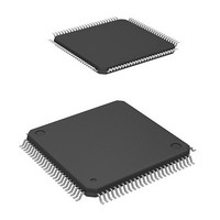
HD64F2239TF20I Renesas Electronics America, HD64F2239TF20I Datasheet - Page 240

HD64F2239TF20I
Manufacturer Part Number
HD64F2239TF20I
Description
MCU 3V 384K I-TEMP 100-TQFP
Manufacturer
Renesas Electronics America
Series
H8® H8S/2200r
Datasheet
1.DF2238RFA6V.pdf
(1048 pages)
Specifications of HD64F2239TF20I
Core Processor
H8S/2000
Core Size
16-Bit
Speed
20MHz
Connectivity
I²C, SCI, SmartCard
Peripherals
DMA, POR, PWM, WDT
Number Of I /o
72
Program Memory Size
384KB (384K x 8)
Program Memory Type
FLASH
Ram Size
32K x 8
Voltage - Supply (vcc/vdd)
2.7 V ~ 3.6 V
Data Converters
A/D 8x10b; D/A 2x8b
Oscillator Type
Internal
Operating Temperature
-40°C ~ 85°C
Package / Case
100-TQFP, 100-VQFP
Lead Free Status / RoHS Status
Contains lead / RoHS non-compliant
Eeprom Size
-
Available stocks
Company
Part Number
Manufacturer
Quantity
Price
Company:
Part Number:
HD64F2239TF20I
Manufacturer:
Renesas Electronics America
Quantity:
10 000
- Current page: 240 of 1048
- Download datasheet (6Mb)
Section 7 Bus Controller
7.4.4
This LSI can output chip select signals (CS7 to CS0) to areas 7 to 0, the signal being driven low
when the corresponding external space area is accessed. Figure 7.3 shows an example of CSn (n =
7 to 0) output timing. Enabling or disabling of the CSn signal is performed by setting the data
direction register (DDR) for the port corresponding to the particular CSn pin.
In ROM-disabled extended mode, the CS0 pin is placed in the output state after a power-on reset.
Pins CS7 to CS1 are placed in the input state after a power-on reset, and so the corresponding
DDR should be set to 1 when outputting signals CS7 to CS1.
In ROM-enabled extended mode, pins CS7 to CS0 are all placed in the input state after a power-on
reset, and so the corresponding DDR should be set to 1 when outputting signals CS7 to CS0. For
details, see section 10, I/O Ports.
7.5
The CPU is driven by a system clock (φ), denoted by the symbol φ. The period from one rising
edge of φ to the next is referred to as a “state”. The memory cycle or bus cycle consists of one,
two, or three states. Different methods are used to access on-chip memory, on-chip peripheral
modules, and the external address space.
Rev. 6.00 Mar. 18, 2010 Page 178 of 982
REJ09B0054-0600
Only the basic bus interface can be used for the area 7.
Chip Select Signals
Basic Timing
Address bus
Figure 7.3 CSn Signal Output Timing (n = 0 to 7)
φ
CSn
T
1
Area n external address
Bus cycle
T
2
T
3
Related parts for HD64F2239TF20I
Image
Part Number
Description
Manufacturer
Datasheet
Request
R

Part Number:
Description:
KIT STARTER FOR M16C/29
Manufacturer:
Renesas Electronics America
Datasheet:

Part Number:
Description:
KIT STARTER FOR R8C/2D
Manufacturer:
Renesas Electronics America
Datasheet:

Part Number:
Description:
R0K33062P STARTER KIT
Manufacturer:
Renesas Electronics America
Datasheet:

Part Number:
Description:
KIT STARTER FOR R8C/23 E8A
Manufacturer:
Renesas Electronics America
Datasheet:

Part Number:
Description:
KIT STARTER FOR R8C/25
Manufacturer:
Renesas Electronics America
Datasheet:

Part Number:
Description:
KIT STARTER H8S2456 SHARPE DSPLY
Manufacturer:
Renesas Electronics America
Datasheet:

Part Number:
Description:
KIT STARTER FOR R8C38C
Manufacturer:
Renesas Electronics America
Datasheet:

Part Number:
Description:
KIT STARTER FOR R8C35C
Manufacturer:
Renesas Electronics America
Datasheet:

Part Number:
Description:
KIT STARTER FOR R8CL3AC+LCD APPS
Manufacturer:
Renesas Electronics America
Datasheet:

Part Number:
Description:
KIT STARTER FOR RX610
Manufacturer:
Renesas Electronics America
Datasheet:

Part Number:
Description:
KIT STARTER FOR R32C/118
Manufacturer:
Renesas Electronics America
Datasheet:

Part Number:
Description:
KIT DEV RSK-R8C/26-29
Manufacturer:
Renesas Electronics America
Datasheet:

Part Number:
Description:
KIT STARTER FOR SH7124
Manufacturer:
Renesas Electronics America
Datasheet:

Part Number:
Description:
KIT STARTER FOR H8SX/1622
Manufacturer:
Renesas Electronics America
Datasheet:

Part Number:
Description:
KIT DEV FOR SH7203
Manufacturer:
Renesas Electronics America
Datasheet:


