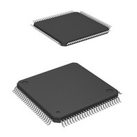
HD64F2239TF20I Renesas Electronics America, HD64F2239TF20I Datasheet - Page 794

HD64F2239TF20I
Manufacturer Part Number
HD64F2239TF20I
Description
MCU 3V 384K I-TEMP 100-TQFP
Manufacturer
Renesas Electronics America
Series
H8® H8S/2200r
Datasheet
1.DF2238RFA6V.pdf
(1048 pages)
Specifications of HD64F2239TF20I
Core Processor
H8S/2000
Core Size
16-Bit
Speed
20MHz
Connectivity
I²C, SCI, SmartCard
Peripherals
DMA, POR, PWM, WDT
Number Of I /o
72
Program Memory Size
384KB (384K x 8)
Program Memory Type
FLASH
Ram Size
32K x 8
Voltage - Supply (vcc/vdd)
2.7 V ~ 3.6 V
Data Converters
A/D 8x10b; D/A 2x8b
Oscillator Type
Internal
Operating Temperature
-40°C ~ 85°C
Package / Case
100-TQFP, 100-VQFP
Lead Free Status / RoHS Status
Contains lead / RoHS non-compliant
Eeprom Size
-
Available stocks
Company
Part Number
Manufacturer
Quantity
Price
Company:
Part Number:
HD64F2239TF20I
Manufacturer:
Renesas Electronics America
Quantity:
10 000
- Current page: 794 of 1048
- Download datasheet (6Mb)
Section 20 Flash Memory (F-ZTAT Version)
Bit
3
2 to 0 —
20.6
When pins are set to on-board programming mode, program/erase/verify operations can be
performed on the on-chip flash memory. There are two on-board programming modes: boot mode
and user program mode. The pin settings for transition to each of these modes are shown in table
20.3. For a diagram of the transitions to the various flash memory modes, see figure 20.2.
Table 20.3 Setting On-Board Programming Modes
Mode Setting
Boot mode
User program mode
20.6.1
Table 20.4 shows the boot mode operations between reset end and branching to the programming
control program.
1. When boot mode is used, the flash memory programming control program must be prepared in
Rev. 6.00 Mar. 18, 2010 Page 732 of 982
REJ09B0054-0600
the host beforehand. Prepare a programming control program in accordance with the
description in section 20.8, Flash Memory Programming/Erasing.
Bit Name
FLSHE
On-Board Programming Modes
Boot Mode
Initial Value R/W
0
All 0
Extended mode
Single-chip mode
Extended mode
Single-chip mode
R/W
R/W
Description
Flash Memory Control Register Enable
Controls for the CPU accessing to the control registers
(FLMCR1, FLMCR2, EBR1, EBR2) of the flash memory.
When this bit is set to 1, the flash memory control
registers can be read/written to. When this bit is cleared
to 0, the flash memory control registers are not selected.
At this time, the contents of the flash memory control
registers are retained.
0: Area at H'FFFFA8 to H'FFFFAC not selected for the
1: Area at H'FFFFA8 to H'FFFFAC selected for the flash
Reserved
Only 0 should be written to these bits.
flash memory control registers.
memory control registers.
FWE
1
1
1
1
MD2
0
0
1
1
MD1
1
1
1
1
MD0
0
1
0
1
Related parts for HD64F2239TF20I
Image
Part Number
Description
Manufacturer
Datasheet
Request
R

Part Number:
Description:
KIT STARTER FOR M16C/29
Manufacturer:
Renesas Electronics America
Datasheet:

Part Number:
Description:
KIT STARTER FOR R8C/2D
Manufacturer:
Renesas Electronics America
Datasheet:

Part Number:
Description:
R0K33062P STARTER KIT
Manufacturer:
Renesas Electronics America
Datasheet:

Part Number:
Description:
KIT STARTER FOR R8C/23 E8A
Manufacturer:
Renesas Electronics America
Datasheet:

Part Number:
Description:
KIT STARTER FOR R8C/25
Manufacturer:
Renesas Electronics America
Datasheet:

Part Number:
Description:
KIT STARTER H8S2456 SHARPE DSPLY
Manufacturer:
Renesas Electronics America
Datasheet:

Part Number:
Description:
KIT STARTER FOR R8C38C
Manufacturer:
Renesas Electronics America
Datasheet:

Part Number:
Description:
KIT STARTER FOR R8C35C
Manufacturer:
Renesas Electronics America
Datasheet:

Part Number:
Description:
KIT STARTER FOR R8CL3AC+LCD APPS
Manufacturer:
Renesas Electronics America
Datasheet:

Part Number:
Description:
KIT STARTER FOR RX610
Manufacturer:
Renesas Electronics America
Datasheet:

Part Number:
Description:
KIT STARTER FOR R32C/118
Manufacturer:
Renesas Electronics America
Datasheet:

Part Number:
Description:
KIT DEV RSK-R8C/26-29
Manufacturer:
Renesas Electronics America
Datasheet:

Part Number:
Description:
KIT STARTER FOR SH7124
Manufacturer:
Renesas Electronics America
Datasheet:

Part Number:
Description:
KIT STARTER FOR H8SX/1622
Manufacturer:
Renesas Electronics America
Datasheet:

Part Number:
Description:
KIT DEV FOR SH7203
Manufacturer:
Renesas Electronics America
Datasheet:


