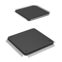
HD64F2239TF20I Renesas Electronics America, HD64F2239TF20I Datasheet - Page 306

HD64F2239TF20I
Manufacturer Part Number
HD64F2239TF20I
Description
MCU 3V 384K I-TEMP 100-TQFP
Manufacturer
Renesas Electronics America
Series
H8® H8S/2200r
Datasheet
1.DF2238RFA6V.pdf
(1048 pages)
Specifications of HD64F2239TF20I
Core Processor
H8S/2000
Core Size
16-Bit
Speed
20MHz
Connectivity
I²C, SCI, SmartCard
Peripherals
DMA, POR, PWM, WDT
Number Of I /o
72
Program Memory Size
384KB (384K x 8)
Program Memory Type
FLASH
Ram Size
32K x 8
Voltage - Supply (vcc/vdd)
2.7 V ~ 3.6 V
Data Converters
A/D 8x10b; D/A 2x8b
Oscillator Type
Internal
Operating Temperature
-40°C ~ 85°C
Package / Case
100-TQFP, 100-VQFP
Lead Free Status / RoHS Status
Contains lead / RoHS non-compliant
Eeprom Size
-
Available stocks
Company
Part Number
Manufacturer
Quantity
Price
Company:
Part Number:
HD64F2239TF20I
Manufacturer:
Renesas Electronics America
Quantity:
10 000
- Current page: 306 of 1048
- Download datasheet (6Mb)
Section 8 DMA Controller (DMAC)
8.5.5
DMAC supports the dual address mode, in which two different cycles are used for reading and
writing, and the single address mode, in which a single cycle is used for both reading and writing.
In dual address mode, the source address and the destination address are specified respectively for
transferring data.
In single address mode, data is transferred between the external space, in which the transfer source
or transfer destination is specified by the address, and the external device that is selected by
DACK strobe regardless of the address. Figure 8.9 shows the data bus in single address mode.
When the data bus is used for reading in single address mode, data is transferred from the external
memory to the external device and the DACK pin functions as the write strobe for the external
device. When the data bus is used for writing in single address mode, data is transferred from the
external device to the external memory and the DACK pin functions as the read strobe for the
external device. Since the direction for the external device cannot be controlled, chose one of
directions described above.
The setting of the bus controller for the external memory area controls the bus cycle in single
address mode. To the external device, DACK is output in synchronization with the address strobe.
For details on the bus cycle, see section 8.5.10, DMA Transfer (Single Address Mode) Bus
Cycles.
In single address mode, do not specify the internal area for the transfer address.
Rev. 6.00 Mar. 18, 2010 Page 244 of 982
REJ09B0054-0600
Single Address Mode
Figure 8.9 Data Bus in Single Address Mode
(High impedance)
This LSI
HWR, LWR
D15 to D0
A23 to A0
DACK
RD
Address bus
(Read)
(Write)
External
memory
External
device
Related parts for HD64F2239TF20I
Image
Part Number
Description
Manufacturer
Datasheet
Request
R

Part Number:
Description:
KIT STARTER FOR M16C/29
Manufacturer:
Renesas Electronics America
Datasheet:

Part Number:
Description:
KIT STARTER FOR R8C/2D
Manufacturer:
Renesas Electronics America
Datasheet:

Part Number:
Description:
R0K33062P STARTER KIT
Manufacturer:
Renesas Electronics America
Datasheet:

Part Number:
Description:
KIT STARTER FOR R8C/23 E8A
Manufacturer:
Renesas Electronics America
Datasheet:

Part Number:
Description:
KIT STARTER FOR R8C/25
Manufacturer:
Renesas Electronics America
Datasheet:

Part Number:
Description:
KIT STARTER H8S2456 SHARPE DSPLY
Manufacturer:
Renesas Electronics America
Datasheet:

Part Number:
Description:
KIT STARTER FOR R8C38C
Manufacturer:
Renesas Electronics America
Datasheet:

Part Number:
Description:
KIT STARTER FOR R8C35C
Manufacturer:
Renesas Electronics America
Datasheet:

Part Number:
Description:
KIT STARTER FOR R8CL3AC+LCD APPS
Manufacturer:
Renesas Electronics America
Datasheet:

Part Number:
Description:
KIT STARTER FOR RX610
Manufacturer:
Renesas Electronics America
Datasheet:

Part Number:
Description:
KIT STARTER FOR R32C/118
Manufacturer:
Renesas Electronics America
Datasheet:

Part Number:
Description:
KIT DEV RSK-R8C/26-29
Manufacturer:
Renesas Electronics America
Datasheet:

Part Number:
Description:
KIT STARTER FOR SH7124
Manufacturer:
Renesas Electronics America
Datasheet:

Part Number:
Description:
KIT STARTER FOR H8SX/1622
Manufacturer:
Renesas Electronics America
Datasheet:

Part Number:
Description:
KIT DEV FOR SH7203
Manufacturer:
Renesas Electronics America
Datasheet:


