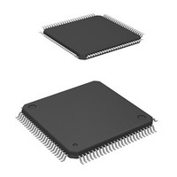
HD64F2239TF20I Renesas Electronics America, HD64F2239TF20I Datasheet - Page 46

HD64F2239TF20I
Manufacturer Part Number
HD64F2239TF20I
Description
MCU 3V 384K I-TEMP 100-TQFP
Manufacturer
Renesas Electronics America
Series
H8® H8S/2200r
Datasheet
1.DF2238RFA6V.pdf
(1048 pages)
Specifications of HD64F2239TF20I
Core Processor
H8S/2000
Core Size
16-Bit
Speed
20MHz
Connectivity
I²C, SCI, SmartCard
Peripherals
DMA, POR, PWM, WDT
Number Of I /o
72
Program Memory Size
384KB (384K x 8)
Program Memory Type
FLASH
Ram Size
32K x 8
Voltage - Supply (vcc/vdd)
2.7 V ~ 3.6 V
Data Converters
A/D 8x10b; D/A 2x8b
Oscillator Type
Internal
Operating Temperature
-40°C ~ 85°C
Package / Case
100-TQFP, 100-VQFP
Lead Free Status / RoHS Status
Contains lead / RoHS non-compliant
Eeprom Size
-
Available stocks
Company
Part Number
Manufacturer
Quantity
Price
Company:
Part Number:
HD64F2239TF20I
Manufacturer:
Renesas Electronics America
Quantity:
10 000
- Current page: 46 of 1048
- Download datasheet (6Mb)
Figure 9.12
Section 10 I/O Ports
Figure 10.1
Section 11 16-Bit Timer Pulse Unit (TPU)
Figure 11.1
Figure 11.2
Figure 11.3
Figure 11.4
Figure 11.5
Figure 11.6
Figure 11.7
Figure 11.8
Figure 11.9
Figure 11.10 Example of Input Capture Operation ................................................................... 403
Figure 11.11 Example of Synchronous Operation Setting Procedure ....................................... 404
Figure 11.12 Example of Synchronous Operation..................................................................... 405
Figure 11.13 Compare Match Buffer Operation........................................................................ 406
Figure 11.14 Input Capture Buffer Operation ........................................................................... 406
Figure 11.15 Example of Buffer Operation Setting Procedure.................................................. 407
Figure 11.16 Example of Buffer Operation (1) ......................................................................... 408
Figure 11.17 Example of Buffer Operation (2) ......................................................................... 409
Figure 11.18 Cascaded Operation Setting Procedure ................................................................ 410
Figure 11.19 Example of Cascaded Operation (1) .................................................................... 410
Figure 11.20 Example of Cascaded Operation (2) .................................................................... 411
Figure 11.21 Example of PWM Mode Setting Procedure ......................................................... 413
Figure 11.22 Example of PWM Mode Operation (1)................................................................ 414
Figure 11.23 Example of PWM Mode Operation (2)................................................................ 414
Figure 11.24 Example of PWM Mode Operation (3)................................................................ 415
Figure 11.25 Example of Phase Counting Mode Setting Procedure ......................................... 417
Figure 11.26 Example of Phase Counting Mode 1 Operation ................................................... 417
Figure 11.27 Example of Phase Counting Mode 2 Operation ................................................... 419
Figure 11.28 Example of Phase Counting Mode 3 Operation ................................................... 420
Figure 11.29 Example of Phase Counting Mode 4 Operation ................................................... 421
Figure 11.30 Phase Counting Mode Application Example ....................................................... 422
Figure 11.31 Count Timing in Internal Clock Operation .......................................................... 426
Figure 11.32 Count Timing in External Clock Operation ......................................................... 427
Figure 11.33 Output Compare Output Timing .......................................................................... 427
Rev. 6.00 Mar. 18, 2010 Page xliv of lx
REJ09B0054-0600
DTC Operation Timing (Example of Chain Transfer) ......................................... 299
Types of Open Drain Outputs .............................................................................. 318
Block Diagram of TPU (H8S/2258 Group, H8S/2239 Group, H8S/2238 Group,
and H8S/2237 Group) .......................................................................................... 362
Block Diagram of TPU (H8S/2227 Group) ......................................................... 363
Example of Counter Operation Setting Procedure ............................................... 398
Free-Running Counter Operation......................................................................... 399
Periodic Counter Operation.................................................................................. 400
Example of Setting Procedure for Waveform Output by Compare Match........... 400
Example of 0 Output/1 Output Operation ............................................................ 401
Example of Toggle Output Operation .................................................................. 401
Example of Setting Procedure for Input Capture Operation ................................ 402
Related parts for HD64F2239TF20I
Image
Part Number
Description
Manufacturer
Datasheet
Request
R

Part Number:
Description:
KIT STARTER FOR M16C/29
Manufacturer:
Renesas Electronics America
Datasheet:

Part Number:
Description:
KIT STARTER FOR R8C/2D
Manufacturer:
Renesas Electronics America
Datasheet:

Part Number:
Description:
R0K33062P STARTER KIT
Manufacturer:
Renesas Electronics America
Datasheet:

Part Number:
Description:
KIT STARTER FOR R8C/23 E8A
Manufacturer:
Renesas Electronics America
Datasheet:

Part Number:
Description:
KIT STARTER FOR R8C/25
Manufacturer:
Renesas Electronics America
Datasheet:

Part Number:
Description:
KIT STARTER H8S2456 SHARPE DSPLY
Manufacturer:
Renesas Electronics America
Datasheet:

Part Number:
Description:
KIT STARTER FOR R8C38C
Manufacturer:
Renesas Electronics America
Datasheet:

Part Number:
Description:
KIT STARTER FOR R8C35C
Manufacturer:
Renesas Electronics America
Datasheet:

Part Number:
Description:
KIT STARTER FOR R8CL3AC+LCD APPS
Manufacturer:
Renesas Electronics America
Datasheet:

Part Number:
Description:
KIT STARTER FOR RX610
Manufacturer:
Renesas Electronics America
Datasheet:

Part Number:
Description:
KIT STARTER FOR R32C/118
Manufacturer:
Renesas Electronics America
Datasheet:

Part Number:
Description:
KIT DEV RSK-R8C/26-29
Manufacturer:
Renesas Electronics America
Datasheet:

Part Number:
Description:
KIT STARTER FOR SH7124
Manufacturer:
Renesas Electronics America
Datasheet:

Part Number:
Description:
KIT STARTER FOR H8SX/1622
Manufacturer:
Renesas Electronics America
Datasheet:

Part Number:
Description:
KIT DEV FOR SH7203
Manufacturer:
Renesas Electronics America
Datasheet:


