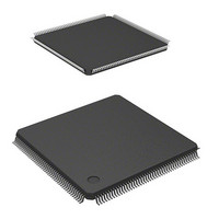
HD6417706F133 Renesas Electronics America, HD6417706F133 Datasheet - Page 216

HD6417706F133
Manufacturer Part Number
HD6417706F133
Description
IC SUPERH MPU ROMLESS 176LQFP
Manufacturer
Renesas Electronics America
Series
SuperH® SH7700r
Datasheet
1.HD6417706F133V.pdf
(751 pages)
Specifications of HD6417706F133
Core Processor
SH-3
Core Size
32-Bit
Speed
133MHz
Connectivity
EBI/EMI, FIFO, SCI, SmartCard
Peripherals
DMA, POR, WDT
Number Of I /o
103
Program Memory Type
ROMless
Ram Size
16K x 8
Voltage - Supply (vcc/vdd)
1.75 V ~ 2.05 V
Oscillator Type
Internal
Operating Temperature
-20°C ~ 75°C
Package / Case
176-LQFP
Lead Free Status / RoHS Status
Contains lead / RoHS non-compliant
Eeprom Size
-
Program Memory Size
-
Data Converters
-
Available stocks
Company
Part Number
Manufacturer
Quantity
Price
Part Number:
HD6417706F133
Manufacturer:
RENESAS/瑞萨
Quantity:
20 000
Company:
Part Number:
HD6417706F133V
Manufacturer:
EDISON
Quantity:
2 000
Company:
Part Number:
HD6417706F133V
Manufacturer:
Renesas Electronics America
Quantity:
10 000
Part Number:
HD6417706F133V
Manufacturer:
RENESAS/瑞萨
Quantity:
20 000
- Current page: 216 of 751
- Download datasheet (5Mb)
Section 8 Bus State Controller (BSC)
8.3
Space Allocation: In the architecture of this LSI, both logical spaces and physical spaces have 32-
bit address spaces. The logical space is divided into five areas by the value of the upper bits of the
address. The physical space is divided into eight areas.
Logical space can be allocated at physical spaces using a memory management unit (MMU). For
details, refer to section 3, Memory Management Unit (MMU), which describes area allocation for
physical spaces.
As listed in table 8.2, this LSI can be connected directly to six areas of memory/PCMCIA
interface, and it outputs chip select signals (CS0, CS2 to CS6, CE2A, CE2B) for each of them.
CS0 is asserted during area 0 access; CS6 is asserted during area 6 access. When PCMCIA
interface is selected in area 5 or 6, in addition to CS5/CS6, CE2A/CE2B are asserted for the
corresponding bytes accessed.
Rev. 5.00 May 29, 2006 page 166 of 698
REJ09B0146-0500
Pin Name
Data enable 2
Data enable 3
Read
Wait
Clock enable
IOIS16
Bus release request
Bus release
acknowledgment
Area Overview
Signal
WE2/DQMUL/
ICIORD
WE3/DQMUU/
ICIOWR
RD
WAIT
CKE
IOIS16
BREQ
BACK
I/O
O
O
O
I
O
I
I
O
Description
When memory other than synchronous DRAM is
used, selects D23 to D16 write strobe signal.
When synchronous DRAM is used, selects D23 to
D16. When PCMCIA is used, strobe signal
indicating I/O read.
When memory other than synchronous DRAM is
used, selects D31 to D24 write strobe signal.
When synchronous DRAM is used, selects D31 to
D24. When PCMCIA is used, strobe signal
indicating I/O write.
Strobe signal indicating read cycle
Wait state request signal
Clock enable control signal of synchronous DRAM
Signal indicating PCMCIA 16-bit I/O. Valid only in
little-endian mode.
Bus release request signal
Bus release acknowledge signal
Related parts for HD6417706F133
Image
Part Number
Description
Manufacturer
Datasheet
Request
R

Part Number:
Description:
KIT STARTER FOR M16C/29
Manufacturer:
Renesas Electronics America
Datasheet:

Part Number:
Description:
KIT STARTER FOR R8C/2D
Manufacturer:
Renesas Electronics America
Datasheet:

Part Number:
Description:
R0K33062P STARTER KIT
Manufacturer:
Renesas Electronics America
Datasheet:

Part Number:
Description:
KIT STARTER FOR R8C/23 E8A
Manufacturer:
Renesas Electronics America
Datasheet:

Part Number:
Description:
KIT STARTER FOR R8C/25
Manufacturer:
Renesas Electronics America
Datasheet:

Part Number:
Description:
KIT STARTER H8S2456 SHARPE DSPLY
Manufacturer:
Renesas Electronics America
Datasheet:

Part Number:
Description:
KIT STARTER FOR R8C38C
Manufacturer:
Renesas Electronics America
Datasheet:

Part Number:
Description:
KIT STARTER FOR R8C35C
Manufacturer:
Renesas Electronics America
Datasheet:

Part Number:
Description:
KIT STARTER FOR R8CL3AC+LCD APPS
Manufacturer:
Renesas Electronics America
Datasheet:

Part Number:
Description:
KIT STARTER FOR RX610
Manufacturer:
Renesas Electronics America
Datasheet:

Part Number:
Description:
KIT STARTER FOR R32C/118
Manufacturer:
Renesas Electronics America
Datasheet:

Part Number:
Description:
KIT DEV RSK-R8C/26-29
Manufacturer:
Renesas Electronics America
Datasheet:

Part Number:
Description:
KIT STARTER FOR SH7124
Manufacturer:
Renesas Electronics America
Datasheet:

Part Number:
Description:
KIT STARTER FOR H8SX/1622
Manufacturer:
Renesas Electronics America
Datasheet:

Part Number:
Description:
KIT DEV FOR SH7203
Manufacturer:
Renesas Electronics America
Datasheet:


