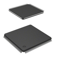
HD6417706F133 Renesas Electronics America, HD6417706F133 Datasheet - Page 477

HD6417706F133
Manufacturer Part Number
HD6417706F133
Description
IC SUPERH MPU ROMLESS 176LQFP
Manufacturer
Renesas Electronics America
Series
SuperH® SH7700r
Datasheet
1.HD6417706F133V.pdf
(751 pages)
Specifications of HD6417706F133
Core Processor
SH-3
Core Size
32-Bit
Speed
133MHz
Connectivity
EBI/EMI, FIFO, SCI, SmartCard
Peripherals
DMA, POR, WDT
Number Of I /o
103
Program Memory Type
ROMless
Ram Size
16K x 8
Voltage - Supply (vcc/vdd)
1.75 V ~ 2.05 V
Oscillator Type
Internal
Operating Temperature
-20°C ~ 75°C
Package / Case
176-LQFP
Lead Free Status / RoHS Status
Contains lead / RoHS non-compliant
Eeprom Size
-
Program Memory Size
-
Data Converters
-
Available stocks
Company
Part Number
Manufacturer
Quantity
Price
Part Number:
HD6417706F133
Manufacturer:
RENESAS/瑞萨
Quantity:
20 000
Company:
Part Number:
HD6417706F133V
Manufacturer:
EDISON
Quantity:
2 000
Company:
Part Number:
HD6417706F133V
Manufacturer:
Renesas Electronics America
Quantity:
10 000
Part Number:
HD6417706F133V
Manufacturer:
RENESAS/瑞萨
Quantity:
20 000
- Current page: 477 of 751
- Download datasheet (5Mb)
15.4
15.4.1
The primary functions of the smart card interface are described below.
1. Each frame consists of 8-bit data and a parity bit.
2. During transmission, the card leaves a guard time of at least 2 etu (elementary time units: the
3. During reception, the card outputs an error signal low level for 1 etu after 10.5 etu has elapsed
4. During transmission, it automatically transmits the same data after allowing at least 2 etu from
5. Only start-stop type asynchronous communication functions are supported; no synchronous
15.4.2
Figure 15.2 shows the pin connection diagram for the smart card interface. During communication
with an IC card, transmission and reception are both carried out over the same data transfer line,
so connect the TxD and RxD pins on the chip. Pull up the data transfer line to the power supply
V
When using the clock generated by the smart card interface on an IC card, input the SCK pin
output to the IC card's CLK pin. This connection is not necessary when the internal clock is used
on the IC card.
Use the chip's port output as the reset signal. Apart from these pins, the power and ground pin
connections are usually also required.
Note: When the IC card is not connected and both RE and TE are set to 1, closed communication
CC
period for 1 bit to transfer) from the end of the parity bit to the start of the next frame.
from the start bit if a parity error was detected.
the time the error signal is sampled.
communication functions are available.
side with a resistor.
is possible and self-diagnosis can be performed.
Operation
Overview
Pin Connections
Rev. 5.00 May 29, 2006 page 427 of 698
Section 15 Smart Card Interface
REJ09B0146-0500
Related parts for HD6417706F133
Image
Part Number
Description
Manufacturer
Datasheet
Request
R

Part Number:
Description:
KIT STARTER FOR M16C/29
Manufacturer:
Renesas Electronics America
Datasheet:

Part Number:
Description:
KIT STARTER FOR R8C/2D
Manufacturer:
Renesas Electronics America
Datasheet:

Part Number:
Description:
R0K33062P STARTER KIT
Manufacturer:
Renesas Electronics America
Datasheet:

Part Number:
Description:
KIT STARTER FOR R8C/23 E8A
Manufacturer:
Renesas Electronics America
Datasheet:

Part Number:
Description:
KIT STARTER FOR R8C/25
Manufacturer:
Renesas Electronics America
Datasheet:

Part Number:
Description:
KIT STARTER H8S2456 SHARPE DSPLY
Manufacturer:
Renesas Electronics America
Datasheet:

Part Number:
Description:
KIT STARTER FOR R8C38C
Manufacturer:
Renesas Electronics America
Datasheet:

Part Number:
Description:
KIT STARTER FOR R8C35C
Manufacturer:
Renesas Electronics America
Datasheet:

Part Number:
Description:
KIT STARTER FOR R8CL3AC+LCD APPS
Manufacturer:
Renesas Electronics America
Datasheet:

Part Number:
Description:
KIT STARTER FOR RX610
Manufacturer:
Renesas Electronics America
Datasheet:

Part Number:
Description:
KIT STARTER FOR R32C/118
Manufacturer:
Renesas Electronics America
Datasheet:

Part Number:
Description:
KIT DEV RSK-R8C/26-29
Manufacturer:
Renesas Electronics America
Datasheet:

Part Number:
Description:
KIT STARTER FOR SH7124
Manufacturer:
Renesas Electronics America
Datasheet:

Part Number:
Description:
KIT STARTER FOR H8SX/1622
Manufacturer:
Renesas Electronics America
Datasheet:

Part Number:
Description:
KIT DEV FOR SH7203
Manufacturer:
Renesas Electronics America
Datasheet:


