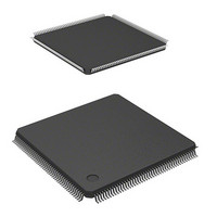
HD6417706F133 Renesas Electronics America, HD6417706F133 Datasheet - Page 463

HD6417706F133
Manufacturer Part Number
HD6417706F133
Description
IC SUPERH MPU ROMLESS 176LQFP
Manufacturer
Renesas Electronics America
Series
SuperH® SH7700r
Datasheet
1.HD6417706F133V.pdf
(751 pages)
Specifications of HD6417706F133
Core Processor
SH-3
Core Size
32-Bit
Speed
133MHz
Connectivity
EBI/EMI, FIFO, SCI, SmartCard
Peripherals
DMA, POR, WDT
Number Of I /o
103
Program Memory Type
ROMless
Ram Size
16K x 8
Voltage - Supply (vcc/vdd)
1.75 V ~ 2.05 V
Oscillator Type
Internal
Operating Temperature
-20°C ~ 75°C
Package / Case
176-LQFP
Lead Free Status / RoHS Status
Contains lead / RoHS non-compliant
Eeprom Size
-
Program Memory Size
-
Data Converters
-
Available stocks
Company
Part Number
Manufacturer
Quantity
Price
Part Number:
HD6417706F133
Manufacturer:
RENESAS/瑞萨
Quantity:
20 000
Company:
Part Number:
HD6417706F133V
Manufacturer:
EDISON
Quantity:
2 000
Company:
Part Number:
HD6417706F133V
Manufacturer:
Renesas Electronics America
Quantity:
10 000
Part Number:
HD6417706F133V
Manufacturer:
RENESAS/瑞萨
Quantity:
20 000
- Current page: 463 of 751
- Download datasheet (5Mb)
In transmitting serial data, the SCI operates as follows:
1. The SCI monitors the TDRE bit in the SCSSR. When TDRE is cleared to 0 the SCI recognizes
2. After loading the data from the SCTDR into the SCTSR, the SCI sets the TDRE bit to 1 and
3. The SCI checks the TDRE bit when it outputs the MSB (bit 7). If TDRE is 0, the SCI loads
4. After the end of serial transmission, the SCK0 pin is held in the high state.
Figure 14.20 shows an example of SCI transmit operation.
that the SCTDR contains new data and loads this data from the SCTDR into the SCTSR.
starts transmitting. If the transmit-data-empty interrupt enable bit (TIE) in the SCSCR is set to
1, the SCI requests a transmit-data-empty interrupt (TXI) at this time.
If clock output mode is selected, the SCI outputs eight synchronous clock pulses. If an external
clock source is selected, the SCI outputs data in synchronization with the input clock. Data are
output from the TxD0 pin in order from the LSB (bit 0) to the MSB (bit 7).
data from the SCTDR into the SCTSR, then begins serial transmission of the next frame. If
TDRE is 1, the SCI sets the TEND bit in the SCSSR to 1, transmits the MSB, then holds the
transmit data pin (TxD0) in the MSB state. If the TEIE in the SCSCR is set to 1, a transmit-end
interrupt (TEI) is requested at this time.
Synchronization
clock
Serial data
TDRE
TEND
TXI interrupt
request
generated
Transfer direction
Figure 14.20 Example of SCI Transmit Operation
Bit 0
LSB
Writes data to TDR
with the TXI interrupt
processing routine
and clears TDRE
bit to 0
Bit 1
1 frame
TXI interrupt
request
generated
Section 14 Serial Communication Interface (SCI)
MSB
Bit 7
Bit 0
Rev. 5.00 May 29, 2006 page 413 of 698
Bit 1
Bit 6
REJ09B0146-0500
TEI interrupt
request
generated
Bit 7
Related parts for HD6417706F133
Image
Part Number
Description
Manufacturer
Datasheet
Request
R

Part Number:
Description:
KIT STARTER FOR M16C/29
Manufacturer:
Renesas Electronics America
Datasheet:

Part Number:
Description:
KIT STARTER FOR R8C/2D
Manufacturer:
Renesas Electronics America
Datasheet:

Part Number:
Description:
R0K33062P STARTER KIT
Manufacturer:
Renesas Electronics America
Datasheet:

Part Number:
Description:
KIT STARTER FOR R8C/23 E8A
Manufacturer:
Renesas Electronics America
Datasheet:

Part Number:
Description:
KIT STARTER FOR R8C/25
Manufacturer:
Renesas Electronics America
Datasheet:

Part Number:
Description:
KIT STARTER H8S2456 SHARPE DSPLY
Manufacturer:
Renesas Electronics America
Datasheet:

Part Number:
Description:
KIT STARTER FOR R8C38C
Manufacturer:
Renesas Electronics America
Datasheet:

Part Number:
Description:
KIT STARTER FOR R8C35C
Manufacturer:
Renesas Electronics America
Datasheet:

Part Number:
Description:
KIT STARTER FOR R8CL3AC+LCD APPS
Manufacturer:
Renesas Electronics America
Datasheet:

Part Number:
Description:
KIT STARTER FOR RX610
Manufacturer:
Renesas Electronics America
Datasheet:

Part Number:
Description:
KIT STARTER FOR R32C/118
Manufacturer:
Renesas Electronics America
Datasheet:

Part Number:
Description:
KIT DEV RSK-R8C/26-29
Manufacturer:
Renesas Electronics America
Datasheet:

Part Number:
Description:
KIT STARTER FOR SH7124
Manufacturer:
Renesas Electronics America
Datasheet:

Part Number:
Description:
KIT STARTER FOR H8SX/1622
Manufacturer:
Renesas Electronics America
Datasheet:

Part Number:
Description:
KIT DEV FOR SH7203
Manufacturer:
Renesas Electronics America
Datasheet:


