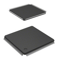
HD6417706F133 Renesas Electronics America, HD6417706F133 Datasheet - Page 425

HD6417706F133
Manufacturer Part Number
HD6417706F133
Description
IC SUPERH MPU ROMLESS 176LQFP
Manufacturer
Renesas Electronics America
Series
SuperH® SH7700r
Datasheet
1.HD6417706F133V.pdf
(751 pages)
Specifications of HD6417706F133
Core Processor
SH-3
Core Size
32-Bit
Speed
133MHz
Connectivity
EBI/EMI, FIFO, SCI, SmartCard
Peripherals
DMA, POR, WDT
Number Of I /o
103
Program Memory Type
ROMless
Ram Size
16K x 8
Voltage - Supply (vcc/vdd)
1.75 V ~ 2.05 V
Oscillator Type
Internal
Operating Temperature
-20°C ~ 75°C
Package / Case
176-LQFP
Lead Free Status / RoHS Status
Contains lead / RoHS non-compliant
Eeprom Size
-
Program Memory Size
-
Data Converters
-
Available stocks
Company
Part Number
Manufacturer
Quantity
Price
Part Number:
HD6417706F133
Manufacturer:
RENESAS/瑞萨
Quantity:
20 000
Company:
Part Number:
HD6417706F133V
Manufacturer:
EDISON
Quantity:
2 000
Company:
Part Number:
HD6417706F133V
Manufacturer:
Renesas Electronics America
Quantity:
10 000
Part Number:
HD6417706F133V
Manufacturer:
RENESAS/瑞萨
Quantity:
20 000
- Current page: 425 of 751
- Download datasheet (5Mb)
Bit
1
0
Bit Name
CKE1
CKE0
Initial Value
0
0
R/W
R/W
R/W
Description
Clock Enable 1 and 0
These bits select the SCI clock source and enable or
disable clock output from the SCK pin. Depending on
the combination of CKE1 and CKE0, the SCK pin can
be used for serial clock output or serial clock input.
The CKE0 setting is valid only in the asynchronous
mode, and only when the SCI is internally clock (CKE1
synchronous mode, or when an external clock source is
selected (CKE1
operating mode in the serial mode register (SCSMR),
set CKE1 and CKE0. For further details on selection of
the SCI clock source, see table 14.9.
00: Internal clock; SCK0 pin is used for input pin (input
01: Internal clock; SCK0 pin is used for clock output. *
01: External clock; SCK0 pin is used for clock input. *
11: External clock; SCK0 pin is used for clock input. *
00: Internal clock; SCK0 pin is used for synchronous
01: Internal clock; SCK0 pin is used for synchronous
01: External clock; SCK0 pin is used for synchronous
11: External clock; SCK0 pin is used for synchronous
Notes: 1. Initial value
0). The CKE0 setting is ignored in the clock
Asynchronous mode
Clock synchronous mode
signal is ignored). *
clock output. *
clock output.
clock input.
clock input.
Section 14 Serial Communication Interface (SCI)
2. The output clock frequency is the same as
3. The input clock frequency is 16 times the bit
the bit rate.
rate.
Rev. 5.00 May 29, 2006 page 375 of 698
1
1). Before selecting the SCI
1
REJ09B0146-0500
3
3
2
Related parts for HD6417706F133
Image
Part Number
Description
Manufacturer
Datasheet
Request
R

Part Number:
Description:
KIT STARTER FOR M16C/29
Manufacturer:
Renesas Electronics America
Datasheet:

Part Number:
Description:
KIT STARTER FOR R8C/2D
Manufacturer:
Renesas Electronics America
Datasheet:

Part Number:
Description:
R0K33062P STARTER KIT
Manufacturer:
Renesas Electronics America
Datasheet:

Part Number:
Description:
KIT STARTER FOR R8C/23 E8A
Manufacturer:
Renesas Electronics America
Datasheet:

Part Number:
Description:
KIT STARTER FOR R8C/25
Manufacturer:
Renesas Electronics America
Datasheet:

Part Number:
Description:
KIT STARTER H8S2456 SHARPE DSPLY
Manufacturer:
Renesas Electronics America
Datasheet:

Part Number:
Description:
KIT STARTER FOR R8C38C
Manufacturer:
Renesas Electronics America
Datasheet:

Part Number:
Description:
KIT STARTER FOR R8C35C
Manufacturer:
Renesas Electronics America
Datasheet:

Part Number:
Description:
KIT STARTER FOR R8CL3AC+LCD APPS
Manufacturer:
Renesas Electronics America
Datasheet:

Part Number:
Description:
KIT STARTER FOR RX610
Manufacturer:
Renesas Electronics America
Datasheet:

Part Number:
Description:
KIT STARTER FOR R32C/118
Manufacturer:
Renesas Electronics America
Datasheet:

Part Number:
Description:
KIT DEV RSK-R8C/26-29
Manufacturer:
Renesas Electronics America
Datasheet:

Part Number:
Description:
KIT STARTER FOR SH7124
Manufacturer:
Renesas Electronics America
Datasheet:

Part Number:
Description:
KIT STARTER FOR H8SX/1622
Manufacturer:
Renesas Electronics America
Datasheet:

Part Number:
Description:
KIT DEV FOR SH7203
Manufacturer:
Renesas Electronics America
Datasheet:


