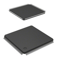
HD6417706F133 Renesas Electronics America, HD6417706F133 Datasheet - Page 39

HD6417706F133
Manufacturer Part Number
HD6417706F133
Description
IC SUPERH MPU ROMLESS 176LQFP
Manufacturer
Renesas Electronics America
Series
SuperH® SH7700r
Datasheet
1.HD6417706F133V.pdf
(751 pages)
Specifications of HD6417706F133
Core Processor
SH-3
Core Size
32-Bit
Speed
133MHz
Connectivity
EBI/EMI, FIFO, SCI, SmartCard
Peripherals
DMA, POR, WDT
Number Of I /o
103
Program Memory Type
ROMless
Ram Size
16K x 8
Voltage - Supply (vcc/vdd)
1.75 V ~ 2.05 V
Oscillator Type
Internal
Operating Temperature
-20°C ~ 75°C
Package / Case
176-LQFP
Lead Free Status / RoHS Status
Contains lead / RoHS non-compliant
Eeprom Size
-
Program Memory Size
-
Data Converters
-
Available stocks
Company
Part Number
Manufacturer
Quantity
Price
Part Number:
HD6417706F133
Manufacturer:
RENESAS/瑞萨
Quantity:
20 000
Company:
Part Number:
HD6417706F133V
Manufacturer:
EDISON
Quantity:
2 000
Company:
Part Number:
HD6417706F133V
Manufacturer:
Renesas Electronics America
Quantity:
10 000
Part Number:
HD6417706F133V
Manufacturer:
RENESAS/瑞萨
Quantity:
20 000
- Current page: 39 of 751
- Download datasheet (5Mb)
Figure 8.31
Figure 8.32
Figure 8.33
Figure 8.34
Figure 8.35
Figure 8.36
Figure 8.37
Figure 8.38
Figure 8.39
Figure 8.40
Figure 8.41
Figure 8.42
Section 9 Direct Memory Access Controller (DMAC)
Figure 9.1
Figure 9.2
Figure 9.3
Figure 9.4
Figure 9.5
Figure 9.6
Figure 9.7
Figure 9.8
Figure 9.9
Figure 9.10
Figure 9.11
Figure 9.12
Figure 9.13
Figure 9.14
Figure 9.15
Figure 9.16
Example of PCMCIA Interface............................................................................ 238
Basic Timing for PCMCIA Memory Card Interface ........................................... 239
Wait Timing for PCMCIA Memory Card Interface............................................. 240
Basic Timing for PCMCIA Memory Card Interface Burst Access...................... 241
Wait Timing for PCMCIA Memory Card Interface Burst Access....................... 242
Basic Timing for PCMCIA I/O Card Interface.................................................... 244
Wait Timing for PCMCIA I/O Card Interface ..................................................... 245
Dynamic Bus Sizing Timing for PCMCIA I/O Card Interface............................ 246
Waits between Access Cycles.............................................................................. 248
Pins A25 to A0 Pull-Up Timing .......................................................................... 249
Pins D31 to D0 Pull-Up Timing (Read Cycle) .................................................... 250
Pins D31 to D0 Pull-Up Timing (Write Cycle).................................................... 250
DMAC Block Diagram ........................................................................................ 253
DMAC Transfer Flowchart.................................................................................. 266
Round-Robin Mode ............................................................................................. 270
Changes in Channel Priority in Round-Robin Mode ........................................... 271
Operation in the Direct Address Mode in the Dual Address Mode ..................... 273
Example of DMA Transfer Timing in the Direct Address Mode in the Dual
Address Mode (Transfer Source: Ordinary Memory, Transfer Destination: Ordinary
Memory) .............................................................................................................. 274
Example of DMA Transfer Timing in the Direct Address Mode in the Dual
Address Mode (16-Byte Transfer, Transfer Source: Ordinary Memory,
Transfer Destination: Ordinary Memory) ............................................................ 275
Example of DMA Transfer Timing in the Direct Address Mode in the Dual
Address Mode (16-Byte Transfer, Transfer Source: Synchronous DRAM,
Transfer Destination: Ordinary Memory) ............................................................ 275
Operation in the Indirect Address mode in the Dual Address Mode
(When the External Memory Space Has a 16-Bit Width).................................... 277
Example of Transfer Timing in the Indirect Address Mode
in the Dual Address Mode ................................................................................... 278
Data Flow in the Single Address Mode ............................................................... 279
Example of DMA Transfer Timing in the Single Address Mode ........................ 280
Example of DMA Transfer Timing in the Single Address Mode
(16-Byte Transfer, External Memory Space (Ordinary Memory)
Device with DACK) ............................................................................................ 281
DMA Transfer Example in the Cycle-Steal Mode............................................... 282
DMA Transfer Example in the Burst Mode......................................................... 282
Bus State when Multiple Channels Are Operating
(Priority Level Is Round-Robin Mode)................................................................ 284
Rev. 5.00 May 29, 2006 page xxxvii of xlviii
External
Related parts for HD6417706F133
Image
Part Number
Description
Manufacturer
Datasheet
Request
R

Part Number:
Description:
KIT STARTER FOR M16C/29
Manufacturer:
Renesas Electronics America
Datasheet:

Part Number:
Description:
KIT STARTER FOR R8C/2D
Manufacturer:
Renesas Electronics America
Datasheet:

Part Number:
Description:
R0K33062P STARTER KIT
Manufacturer:
Renesas Electronics America
Datasheet:

Part Number:
Description:
KIT STARTER FOR R8C/23 E8A
Manufacturer:
Renesas Electronics America
Datasheet:

Part Number:
Description:
KIT STARTER FOR R8C/25
Manufacturer:
Renesas Electronics America
Datasheet:

Part Number:
Description:
KIT STARTER H8S2456 SHARPE DSPLY
Manufacturer:
Renesas Electronics America
Datasheet:

Part Number:
Description:
KIT STARTER FOR R8C38C
Manufacturer:
Renesas Electronics America
Datasheet:

Part Number:
Description:
KIT STARTER FOR R8C35C
Manufacturer:
Renesas Electronics America
Datasheet:

Part Number:
Description:
KIT STARTER FOR R8CL3AC+LCD APPS
Manufacturer:
Renesas Electronics America
Datasheet:

Part Number:
Description:
KIT STARTER FOR RX610
Manufacturer:
Renesas Electronics America
Datasheet:

Part Number:
Description:
KIT STARTER FOR R32C/118
Manufacturer:
Renesas Electronics America
Datasheet:

Part Number:
Description:
KIT DEV RSK-R8C/26-29
Manufacturer:
Renesas Electronics America
Datasheet:

Part Number:
Description:
KIT STARTER FOR SH7124
Manufacturer:
Renesas Electronics America
Datasheet:

Part Number:
Description:
KIT STARTER FOR H8SX/1622
Manufacturer:
Renesas Electronics America
Datasheet:

Part Number:
Description:
KIT DEV FOR SH7203
Manufacturer:
Renesas Electronics America
Datasheet:


