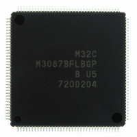
M3087BFLBGP#U5 Renesas Electronics America, M3087BFLBGP#U5 Datasheet - Page 129

M3087BFLBGP#U5
Manufacturer Part Number
M3087BFLBGP#U5
Description
IC M32C/87 MCU FLASH 144LQFP
Manufacturer
Renesas Electronics America
Series
M16C™ M32C/80r
Datasheet
1.M3087BFLGPU3.pdf
(629 pages)
Specifications of M3087BFLBGP#U5
Core Processor
M32C/80
Core Size
16/32-Bit
Speed
32MHz
Connectivity
EBI/EMI, I²C, IEBus, IrDA, SIO, UART/USART
Peripherals
DMA, POR, PWM, WDT
Number Of I /o
121
Program Memory Size
1MB (1M x 8)
Program Memory Type
FLASH
Ram Size
48K x 8
Voltage - Supply (vcc/vdd)
3 V ~ 5.5 V
Data Converters
A/D 34x10b, D/A 2x8b
Oscillator Type
Internal
Operating Temperature
-20°C ~ 85°C
Package / Case
144-LQFP
For Use With
R0K330879S001BE - KIT DEV RSK M32C/87R0K330879S000BE - KIT DEV RSK M32C/87
Lead Free Status / RoHS Status
Lead free / RoHS Compliant
Eeprom Size
-
Available stocks
Company
Part Number
Manufacturer
Quantity
Price
Part Number:
M3087BFLBGP#U5M3087BFLBGP#U3
Manufacturer:
Renesas Electronics America
Quantity:
10 000
- Current page: 129 of 629
- Download datasheet (16Mb)
M32C/87 Group (M32C/87, M32C/87A, M32C/87B)
REJ09B0180-0151 Rev.1.51 Jul 31, 2008
Page 105 of 587
10. Protection
The function protects important registers from being inadvertently overwritten in case of a program crash. Figure 10.1
shows the PRCR register.
The PRC2 bit in the PRCR register becomes 0 (write disable) by a write to the SFR area after the PRC2 bit is set to 1
(write enable). Set the PD9 or PS3 register immediately after the PRC2 bit is set to 1. Do not generate an interrupt or a
DMA or DMACII transfer between these two instructions. Bits PRC0, PRC1, and PRC3 do not become 0
automatically even after a write to the SFR area. Set bits PRC0, PRC1, and PRC3 to 0 by a program.
Figure 10.1
Protect Register
b7 b6 b5 b4
NOTES:
1. Bits PRC0, PRC1, and PRC3 do not become 0 automatically even after a write to the SFR area. Set bits PRC0, PRC1, and
2. The PRC2 bit becomes 0 by a write to the SFR area after the PRC2 bit is set to 1.
PRC3 to 0 by a program.
b3
b2
PRCR Register
b1
b0
Bit Symbol
(b7-b4)
PRC0
PRC1
PRC2
PRC3
Symbol
PRCR
−
Protect bit 0
Protect bit 1
Protect bit 2
Protect bit 3
Unimplemented.
Write 0. Read as undefined value.
Bit Name
(1)
(1)
(2)
(1)
Address
000Ah
Writing to registers CM0, CM1, CM2, MCD,
PLC0, and PLC1 is enabled
0: Write disable
1: Write enable
Writing to registers PM0, PM1, PM2, INVC0,
and INVC1 is enabled
0: Write disable
1: Write enable
Writing to registers PD9 and PS3 is enabled
0: Write disable
1: Write enable
Writing to registers VCR2 and D4INT is enabled
0: Write disable
1: Write enable
Function
After Reset
XXXX 0000b
10. Protection
RW
RW
RW
RW
RW
−
Related parts for M3087BFLBGP#U5
Image
Part Number
Description
Manufacturer
Datasheet
Request
R

Part Number:
Description:
KIT STARTER FOR M16C/29
Manufacturer:
Renesas Electronics America
Datasheet:

Part Number:
Description:
KIT STARTER FOR R8C/2D
Manufacturer:
Renesas Electronics America
Datasheet:

Part Number:
Description:
R0K33062P STARTER KIT
Manufacturer:
Renesas Electronics America
Datasheet:

Part Number:
Description:
KIT STARTER FOR R8C/23 E8A
Manufacturer:
Renesas Electronics America
Datasheet:

Part Number:
Description:
KIT STARTER FOR R8C/25
Manufacturer:
Renesas Electronics America
Datasheet:

Part Number:
Description:
KIT STARTER H8S2456 SHARPE DSPLY
Manufacturer:
Renesas Electronics America
Datasheet:

Part Number:
Description:
KIT STARTER FOR R8C38C
Manufacturer:
Renesas Electronics America
Datasheet:

Part Number:
Description:
KIT STARTER FOR R8C35C
Manufacturer:
Renesas Electronics America
Datasheet:

Part Number:
Description:
KIT STARTER FOR R8CL3AC+LCD APPS
Manufacturer:
Renesas Electronics America
Datasheet:

Part Number:
Description:
KIT STARTER FOR RX610
Manufacturer:
Renesas Electronics America
Datasheet:

Part Number:
Description:
KIT STARTER FOR R32C/118
Manufacturer:
Renesas Electronics America
Datasheet:

Part Number:
Description:
KIT DEV RSK-R8C/26-29
Manufacturer:
Renesas Electronics America
Datasheet:

Part Number:
Description:
KIT STARTER FOR SH7124
Manufacturer:
Renesas Electronics America
Datasheet:

Part Number:
Description:
KIT STARTER FOR H8SX/1622
Manufacturer:
Renesas Electronics America
Datasheet:

Part Number:
Description:
KIT DEV FOR SH7203
Manufacturer:
Renesas Electronics America
Datasheet:


