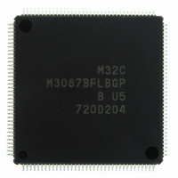
M3087BFLBGP#U5 Renesas Electronics America, M3087BFLBGP#U5 Datasheet - Page 171

M3087BFLBGP#U5
Manufacturer Part Number
M3087BFLBGP#U5
Description
IC M32C/87 MCU FLASH 144LQFP
Manufacturer
Renesas Electronics America
Series
M16C™ M32C/80r
Datasheet
1.M3087BFLGPU3.pdf
(629 pages)
Specifications of M3087BFLBGP#U5
Core Processor
M32C/80
Core Size
16/32-Bit
Speed
32MHz
Connectivity
EBI/EMI, I²C, IEBus, IrDA, SIO, UART/USART
Peripherals
DMA, POR, PWM, WDT
Number Of I /o
121
Program Memory Size
1MB (1M x 8)
Program Memory Type
FLASH
Ram Size
48K x 8
Voltage - Supply (vcc/vdd)
3 V ~ 5.5 V
Data Converters
A/D 34x10b, D/A 2x8b
Oscillator Type
Internal
Operating Temperature
-20°C ~ 85°C
Package / Case
144-LQFP
For Use With
R0K330879S001BE - KIT DEV RSK M32C/87R0K330879S000BE - KIT DEV RSK M32C/87
Lead Free Status / RoHS Status
Lead free / RoHS Compliant
Eeprom Size
-
Available stocks
Company
Part Number
Manufacturer
Quantity
Price
Part Number:
M3087BFLBGP#U5M3087BFLBGP#U3
Manufacturer:
Renesas Electronics America
Quantity:
10 000
- Current page: 171 of 629
- Download datasheet (16Mb)
M32C/87 Group (M32C/87, M32C/87A, M32C/87B)
REJ09B0180-0151 Rev.1.51 Jul 31, 2008
Page 147 of 587
Figure 13.8
<When using repeat transfer>
<When using repeat transfer>
i = 2, 3
NOTES:
1. When setting the DMiSL register, write a 1 to the DRQ bit.
2. The register bank 1 and high-speed interrupt cannot be used when using DMA2 and DMA3.
3. When the INT interrupts are selected as a DMA request source, do not write a 1 to the DCTi register. If the DCTi register is
4. Wait six CPU clock cycles or more by a program to set bits MDi1 and MDi0 to 01b or 11b after setting the DMiSL register.
5. When a DMA transfer is started by the software trigger, set both the DSR and DRQ bit in the DMiSL register to 1 at the
DMD1 register: bits MD21 and MD20 = 00b
DMiSL register: bits DSEL4 to DSEL0
B flag = 1
DMA2 (A0) register or DMA3 (A1) register
DSA2 (SB) register or DSA3 (FB) register
DRA2 (SVP) register or DRA3 (VCT) register
DCT2 (R0) register or DCT3 (R1) register
DRC2 (R2) register or DRC3 (R3) register
B flag = 0
DMD1 register: bits MD21 and MD20
1, do not generate a DMA request when writing 01b or 11b to bits MDi1 and MDi0.
same time.
used as DMAi request source
used as DMAi request source
Start the peripheral function
Register Settings When Using DMA2 or DMA3
Set the peripheral function
bits MD31 and MD30 = 00b
BW2 bit
RW2 bit
bits MD31 and MD30
BW3 bit
RW3 bit
DSR bit = 0
DRQ bit = 1
Start
End
Set the control registers of the peripheral function,
but do not yet start.
DMA disabled for channel 2
DMA disabled for channel 3
DMA request source select bits
DMA requested
Select register bank 1
Set an incremented source address or
incremented destination address
Set a fixed source address or
fixed destination address
Set an incremented source address or
incremented destination address
Set the number of transfer
Set the number of transfer, which is to be
reloaded
Select register bank 0
Transfer mode select bits for channel 2
Transfer unit select bit for channel 2
Transfer direction select bit for channel 2
Transfer mode select bits for channel 3
Transfer unit select bit for channel 3
Transfer direction select bit for channel 3
(note 5)
(2)
(2)
(3)
Write with LDC instruction
Write with MOV instruction
Write with LDC instruction
Write with LDC instruction
Write with MOV instruction
Write with MOV instruction
Write with LDC instruction
(note 4)
(note 1)
13. DMAC
Related parts for M3087BFLBGP#U5
Image
Part Number
Description
Manufacturer
Datasheet
Request
R

Part Number:
Description:
KIT STARTER FOR M16C/29
Manufacturer:
Renesas Electronics America
Datasheet:

Part Number:
Description:
KIT STARTER FOR R8C/2D
Manufacturer:
Renesas Electronics America
Datasheet:

Part Number:
Description:
R0K33062P STARTER KIT
Manufacturer:
Renesas Electronics America
Datasheet:

Part Number:
Description:
KIT STARTER FOR R8C/23 E8A
Manufacturer:
Renesas Electronics America
Datasheet:

Part Number:
Description:
KIT STARTER FOR R8C/25
Manufacturer:
Renesas Electronics America
Datasheet:

Part Number:
Description:
KIT STARTER H8S2456 SHARPE DSPLY
Manufacturer:
Renesas Electronics America
Datasheet:

Part Number:
Description:
KIT STARTER FOR R8C38C
Manufacturer:
Renesas Electronics America
Datasheet:

Part Number:
Description:
KIT STARTER FOR R8C35C
Manufacturer:
Renesas Electronics America
Datasheet:

Part Number:
Description:
KIT STARTER FOR R8CL3AC+LCD APPS
Manufacturer:
Renesas Electronics America
Datasheet:

Part Number:
Description:
KIT STARTER FOR RX610
Manufacturer:
Renesas Electronics America
Datasheet:

Part Number:
Description:
KIT STARTER FOR R32C/118
Manufacturer:
Renesas Electronics America
Datasheet:

Part Number:
Description:
KIT DEV RSK-R8C/26-29
Manufacturer:
Renesas Electronics America
Datasheet:

Part Number:
Description:
KIT STARTER FOR SH7124
Manufacturer:
Renesas Electronics America
Datasheet:

Part Number:
Description:
KIT STARTER FOR H8SX/1622
Manufacturer:
Renesas Electronics America
Datasheet:

Part Number:
Description:
KIT DEV FOR SH7203
Manufacturer:
Renesas Electronics America
Datasheet:


