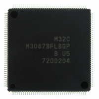
M3087BFLBGP#U5 Renesas Electronics America, M3087BFLBGP#U5 Datasheet - Page 150

M3087BFLBGP#U5
Manufacturer Part Number
M3087BFLBGP#U5
Description
IC M32C/87 MCU FLASH 144LQFP
Manufacturer
Renesas Electronics America
Series
M16C™ M32C/80r
Datasheet
1.M3087BFLGPU3.pdf
(629 pages)
Specifications of M3087BFLBGP#U5
Core Processor
M32C/80
Core Size
16/32-Bit
Speed
32MHz
Connectivity
EBI/EMI, I²C, IEBus, IrDA, SIO, UART/USART
Peripherals
DMA, POR, PWM, WDT
Number Of I /o
121
Program Memory Size
1MB (1M x 8)
Program Memory Type
FLASH
Ram Size
48K x 8
Voltage - Supply (vcc/vdd)
3 V ~ 5.5 V
Data Converters
A/D 34x10b, D/A 2x8b
Oscillator Type
Internal
Operating Temperature
-20°C ~ 85°C
Package / Case
144-LQFP
For Use With
R0K330879S001BE - KIT DEV RSK M32C/87R0K330879S000BE - KIT DEV RSK M32C/87
Lead Free Status / RoHS Status
Lead free / RoHS Compliant
Eeprom Size
-
Available stocks
Company
Part Number
Manufacturer
Quantity
Price
Part Number:
M3087BFLBGP#U5M3087BFLBGP#U3
Manufacturer:
Renesas Electronics America
Quantity:
10 000
- Current page: 150 of 629
- Download datasheet (16Mb)
M32C/87 Group (M32C/87, M32C/87A, M32C/87B)
REJ09B0180-0151 Rev.1.51 Jul 31, 2008
Page 126 of 587
11.8
11.9
Figure 11.15
The NMI interrupt is non-maskable. The NMI interrupt occurs when a signal applied to the P8_5/NMI pin changes
from “H” level to “L” level. A read from the P8_5 bit in the P8 register returns the input level of the NMI pin.
When the NMI interrupt is not used, connect the NMI pin to VCC1 via a resistor (pull-up). Each “H” or “L” width
of the signal applied to the NMI pin must be 2 CPU clock cycles + 300 ns or more.
The IR bit in the KUPIC register becomes 1 when an falling edge is detected at any of the pins P10_4 to P10_7 set
to input mode. The key input interrupt can also be used as key-on wake-up function to exit wait mode or stop mode.
To use the key input interrupt, do not use pins P10_4 to P10_7 as A/D input. Figure 11.15 shows a block diagram of
the key input interrupt. When an “L” signal is applied to one of the pins P10_4 to P10_7 in input mode, a falling
edge detected at the other pins is not recognized as an interrupt request signal.
When the PSC_7 bit in the PSC register is set to 1 (AN_4 to AN_7), the input buffer for the port and the key input
interrupt is disconnected. Therefore, the pin level cannot be obtained by reading the Port P10 register in input
mode. Also, the IR bit in the KUPIC register does not become 1 even if a falling edge is detected at pins KI0 to
KI3.
P10_7/KI3
P10_6/KI2
P10_5/KI1
P10_4/KI0
transistor
Key Input Interrupt
NMI Interrupt
Pull-up
Key Input Interrupt Block Diagram
transistor
transistor
transistor
Pull-up
Pull-up
Pull-up
PSC_7 bit
PD10_7 bit
PD10_6 bit
PD10_5 bit
PD10_4 bit
PD10_7 bit
PU31 bit
PD10_4 to PD10_7: Bits in the PD10 register
PSC_7: Bit in the PSC register
PU31: Bit in the PUR3 register
Key input interrupt request
11. Interrupts
Related parts for M3087BFLBGP#U5
Image
Part Number
Description
Manufacturer
Datasheet
Request
R

Part Number:
Description:
KIT STARTER FOR M16C/29
Manufacturer:
Renesas Electronics America
Datasheet:

Part Number:
Description:
KIT STARTER FOR R8C/2D
Manufacturer:
Renesas Electronics America
Datasheet:

Part Number:
Description:
R0K33062P STARTER KIT
Manufacturer:
Renesas Electronics America
Datasheet:

Part Number:
Description:
KIT STARTER FOR R8C/23 E8A
Manufacturer:
Renesas Electronics America
Datasheet:

Part Number:
Description:
KIT STARTER FOR R8C/25
Manufacturer:
Renesas Electronics America
Datasheet:

Part Number:
Description:
KIT STARTER H8S2456 SHARPE DSPLY
Manufacturer:
Renesas Electronics America
Datasheet:

Part Number:
Description:
KIT STARTER FOR R8C38C
Manufacturer:
Renesas Electronics America
Datasheet:

Part Number:
Description:
KIT STARTER FOR R8C35C
Manufacturer:
Renesas Electronics America
Datasheet:

Part Number:
Description:
KIT STARTER FOR R8CL3AC+LCD APPS
Manufacturer:
Renesas Electronics America
Datasheet:

Part Number:
Description:
KIT STARTER FOR RX610
Manufacturer:
Renesas Electronics America
Datasheet:

Part Number:
Description:
KIT STARTER FOR R32C/118
Manufacturer:
Renesas Electronics America
Datasheet:

Part Number:
Description:
KIT DEV RSK-R8C/26-29
Manufacturer:
Renesas Electronics America
Datasheet:

Part Number:
Description:
KIT STARTER FOR SH7124
Manufacturer:
Renesas Electronics America
Datasheet:

Part Number:
Description:
KIT STARTER FOR H8SX/1622
Manufacturer:
Renesas Electronics America
Datasheet:

Part Number:
Description:
KIT DEV FOR SH7203
Manufacturer:
Renesas Electronics America
Datasheet:


