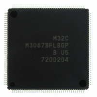
M3087BFLBGP#U5 Renesas Electronics America, M3087BFLBGP#U5 Datasheet - Page 143

M3087BFLBGP#U5
Manufacturer Part Number
M3087BFLBGP#U5
Description
IC M32C/87 MCU FLASH 144LQFP
Manufacturer
Renesas Electronics America
Series
M16C™ M32C/80r
Datasheet
1.M3087BFLGPU3.pdf
(629 pages)
Specifications of M3087BFLBGP#U5
Core Processor
M32C/80
Core Size
16/32-Bit
Speed
32MHz
Connectivity
EBI/EMI, I²C, IEBus, IrDA, SIO, UART/USART
Peripherals
DMA, POR, PWM, WDT
Number Of I /o
121
Program Memory Size
1MB (1M x 8)
Program Memory Type
FLASH
Ram Size
48K x 8
Voltage - Supply (vcc/vdd)
3 V ~ 5.5 V
Data Converters
A/D 34x10b, D/A 2x8b
Oscillator Type
Internal
Operating Temperature
-20°C ~ 85°C
Package / Case
144-LQFP
For Use With
R0K330879S001BE - KIT DEV RSK M32C/87R0K330879S000BE - KIT DEV RSK M32C/87
Lead Free Status / RoHS Status
Lead free / RoHS Compliant
Eeprom Size
-
Available stocks
Company
Part Number
Manufacturer
Quantity
Price
Part Number:
M3087BFLBGP#U5M3087BFLBGP#U3
Manufacturer:
Renesas Electronics America
Quantity:
10 000
- Current page: 143 of 629
- Download datasheet (16Mb)
M32C/87 Group (M32C/87, M32C/87A, M32C/87B)
REJ09B0180-0151 Rev.1.51 Jul 31, 2008
Page 119 of 587
Figure 11.8
11.6.5
Table 11.6
11.6.6
Watchdog timer, NMI, oscillation stop detection, Vdet4 detection,
DMACII end-of-transfer interrupt
Software, address match
Address
m - 6
m - 5
m - 4
m - 3
m - 2
m - 1
m
m + 1
When a peripheral function interrupt request is acknowledged, the priority level for the acknowledged interrupt
becomes the IPL level in the flag register.
Software interrupts and special interrupts have no interrupt priority level. If an interrupt that has no interrupt
priority level occurs, the value shown in Table 11.6 becomes the IPL level.
In the interrupt sequence, values of the FLG register and PC are saved to the stack.
Figure 11.8 shows the stack states before and after an interrupt request is acknowledged.
The other necessary registers are saved by a program at the beginning of the interrupt routine. The PUSHM
instruction can save multiple registers
Refer to 11.4 High-Speed Interrupt for the high-speed interrupt.
NOTE:
1. Selectable from registers R0, R1, R2, R3, A0, A1, SB, and FB.
MSB
Stack state before an interrupt
request is acknowledged
IPL Change when Interrupt Request is Acknowledged
Saving a Register
Previous stack
Previous stack
Interrupts without Interrupt Priority Levels and IPL
Stack States Before and After Acknowledgement of Interrupt Request
contents
contents
Stack
Interrupt Source
LSB
[SP]
SP value before
an interrupt is
generated
(1)
in the register bank currently used.
Address
m - 6
m - 5
m - 4
m - 3
m - 2
m - 1
m
m + 1
MSB
Stack state before an interrupt
request is acknowledged
Previous stack
Previous stack
contents
contents
FLGH
Stack
FLGL
PCM
PCH
PCL
00h
Not changed
LSB
IPL level
7
[SP]
New SP value
PCL: 8 low-order bits of PC
PCM: 8 middle-order bits of PC
PCH: 8 high-order bits of PC
FLGL: 8 low-order bits of FLG
FLGH: 8 high-order bits of FLG
11. Interrupts
Related parts for M3087BFLBGP#U5
Image
Part Number
Description
Manufacturer
Datasheet
Request
R

Part Number:
Description:
KIT STARTER FOR M16C/29
Manufacturer:
Renesas Electronics America
Datasheet:

Part Number:
Description:
KIT STARTER FOR R8C/2D
Manufacturer:
Renesas Electronics America
Datasheet:

Part Number:
Description:
R0K33062P STARTER KIT
Manufacturer:
Renesas Electronics America
Datasheet:

Part Number:
Description:
KIT STARTER FOR R8C/23 E8A
Manufacturer:
Renesas Electronics America
Datasheet:

Part Number:
Description:
KIT STARTER FOR R8C/25
Manufacturer:
Renesas Electronics America
Datasheet:

Part Number:
Description:
KIT STARTER H8S2456 SHARPE DSPLY
Manufacturer:
Renesas Electronics America
Datasheet:

Part Number:
Description:
KIT STARTER FOR R8C38C
Manufacturer:
Renesas Electronics America
Datasheet:

Part Number:
Description:
KIT STARTER FOR R8C35C
Manufacturer:
Renesas Electronics America
Datasheet:

Part Number:
Description:
KIT STARTER FOR R8CL3AC+LCD APPS
Manufacturer:
Renesas Electronics America
Datasheet:

Part Number:
Description:
KIT STARTER FOR RX610
Manufacturer:
Renesas Electronics America
Datasheet:

Part Number:
Description:
KIT STARTER FOR R32C/118
Manufacturer:
Renesas Electronics America
Datasheet:

Part Number:
Description:
KIT DEV RSK-R8C/26-29
Manufacturer:
Renesas Electronics America
Datasheet:

Part Number:
Description:
KIT STARTER FOR SH7124
Manufacturer:
Renesas Electronics America
Datasheet:

Part Number:
Description:
KIT STARTER FOR H8SX/1622
Manufacturer:
Renesas Electronics America
Datasheet:

Part Number:
Description:
KIT DEV FOR SH7203
Manufacturer:
Renesas Electronics America
Datasheet:


