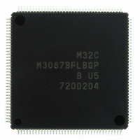
M3087BFLBGP#U5 Renesas Electronics America, M3087BFLBGP#U5 Datasheet - Page 323

M3087BFLBGP#U5
Manufacturer Part Number
M3087BFLBGP#U5
Description
IC M32C/87 MCU FLASH 144LQFP
Manufacturer
Renesas Electronics America
Series
M16C™ M32C/80r
Datasheet
1.M3087BFLGPU3.pdf
(629 pages)
Specifications of M3087BFLBGP#U5
Core Processor
M32C/80
Core Size
16/32-Bit
Speed
32MHz
Connectivity
EBI/EMI, I²C, IEBus, IrDA, SIO, UART/USART
Peripherals
DMA, POR, PWM, WDT
Number Of I /o
121
Program Memory Size
1MB (1M x 8)
Program Memory Type
FLASH
Ram Size
48K x 8
Voltage - Supply (vcc/vdd)
3 V ~ 5.5 V
Data Converters
A/D 34x10b, D/A 2x8b
Oscillator Type
Internal
Operating Temperature
-20°C ~ 85°C
Package / Case
144-LQFP
For Use With
R0K330879S001BE - KIT DEV RSK M32C/87R0K330879S000BE - KIT DEV RSK M32C/87
Lead Free Status / RoHS Status
Lead free / RoHS Compliant
Eeprom Size
-
Available stocks
Company
Part Number
Manufacturer
Quantity
Price
Part Number:
M3087BFLBGP#U5M3087BFLBGP#U3
Manufacturer:
Renesas Electronics America
Quantity:
10 000
- Current page: 323 of 629
- Download datasheet (16Mb)
M32C/87 Group (M32C/87, M32C/87A, M32C/87B)
REJ09B0180-0151 Rev.1.51 Jul 31, 2008
Page 299 of 587
Figure 18.6
A/D0 Control Register 4
A/D0 Register i
b15
0 0
b7
0
b6 b5 b4
0
0
NOTES:
NOTES:
0
0
1. If the AD0CON4 register is rewritten during A/D conversion, the conversion result will be incorrect.
2. Do not set bits MPS11 and MPS10 to 01b in the 100-pin package.
3. Bits MPS11 and MPS10 cannot be set to 10b or 11b in memory expansion mode or microprocessor mode.
4. When the MSS bit in the AD0CON3 register is set to 0 (multi-port sweep mode not used), set bits MPS11 and MPS10 to 00b.
1. When the AD0i register is read by a program in DMAC operating mode, the conversion result is incorrect.
2. If the next A/D conversion result is stored before reading the previous result in the AD0i register, the result will be incorrect.
3. Only AD00 register is enabled in DMAC operating mode. The contents of other registers are undefined.
4. When using both DMAC operating mode and 10-bit mode, select a 16-bit transfer for DMAC.
0
When the MSS bit is set to 1 (multi-port sweep mode used), set bits MPS11 and MPS10 to other than 00b.
0
0
b8
b3
b7
b2
AD0CON4 Register, AD00 to AD07 Registers
b1
0
b0
0
b0
(1, 2, 3, 4)
8 low-order bits of A/D conversion result
In 10-bit mode: 2 high-order bits of A/D conversion result
In 8-bit mode: Read as 0.
Reserved bits. Read as 0.
Bit Symbol
(b1-b0)
MPS10
MPS11
(b7-b4)
Symbol
AD0CON4
Symbol
AD00
AD01 to AD03
AD04 to AD06
AD07
−
−
(i = 0 to 7)
(1)
Reserved bits
Multi-port sweep port
select bits
Reserved bits
(2, 3)
Bit Name
Address
0381h - 0380h
0383h - 0382h, 0385h - 0384h, 0387h - 0386h
0389h - 0388h, 038Bh - 038Ah, 038Dh - 038Ch
038Fh - 038Eh
Address
0392h
Function
Set to 0.
Read as undefined value.
b3 b2
0 0: (Note 4)
0 1: AN_0 to AN_7, AN15_0 to AN15_7
1 0: AN_0 to AN_7, AN0_0 to AN0_7
1 1: AN_0 to AN_7, AN2_0 to AN2_7
Set to 0.
Read as undefined value.
Function
00000000 XXXXXXXXb
00000000 XXXXXXXXb
00000000 XXXXXXXXb
00000000 XXXXXXXXb
After Reset
After Reset
XXXX 00XXb
18. A/D Converter
RW
RW
RW
RW
RW
RW
RO
RO
RO
Related parts for M3087BFLBGP#U5
Image
Part Number
Description
Manufacturer
Datasheet
Request
R

Part Number:
Description:
KIT STARTER FOR M16C/29
Manufacturer:
Renesas Electronics America
Datasheet:

Part Number:
Description:
KIT STARTER FOR R8C/2D
Manufacturer:
Renesas Electronics America
Datasheet:

Part Number:
Description:
R0K33062P STARTER KIT
Manufacturer:
Renesas Electronics America
Datasheet:

Part Number:
Description:
KIT STARTER FOR R8C/23 E8A
Manufacturer:
Renesas Electronics America
Datasheet:

Part Number:
Description:
KIT STARTER FOR R8C/25
Manufacturer:
Renesas Electronics America
Datasheet:

Part Number:
Description:
KIT STARTER H8S2456 SHARPE DSPLY
Manufacturer:
Renesas Electronics America
Datasheet:

Part Number:
Description:
KIT STARTER FOR R8C38C
Manufacturer:
Renesas Electronics America
Datasheet:

Part Number:
Description:
KIT STARTER FOR R8C35C
Manufacturer:
Renesas Electronics America
Datasheet:

Part Number:
Description:
KIT STARTER FOR R8CL3AC+LCD APPS
Manufacturer:
Renesas Electronics America
Datasheet:

Part Number:
Description:
KIT STARTER FOR RX610
Manufacturer:
Renesas Electronics America
Datasheet:

Part Number:
Description:
KIT STARTER FOR R32C/118
Manufacturer:
Renesas Electronics America
Datasheet:

Part Number:
Description:
KIT DEV RSK-R8C/26-29
Manufacturer:
Renesas Electronics America
Datasheet:

Part Number:
Description:
KIT STARTER FOR SH7124
Manufacturer:
Renesas Electronics America
Datasheet:

Part Number:
Description:
KIT STARTER FOR H8SX/1622
Manufacturer:
Renesas Electronics America
Datasheet:

Part Number:
Description:
KIT DEV FOR SH7203
Manufacturer:
Renesas Electronics America
Datasheet:


