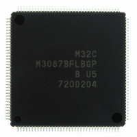
M3087BFLBGP#U5 Renesas Electronics America, M3087BFLBGP#U5 Datasheet - Page 231

M3087BFLBGP#U5
Manufacturer Part Number
M3087BFLBGP#U5
Description
IC M32C/87 MCU FLASH 144LQFP
Manufacturer
Renesas Electronics America
Series
M16C™ M32C/80r
Datasheet
1.M3087BFLGPU3.pdf
(629 pages)
Specifications of M3087BFLBGP#U5
Core Processor
M32C/80
Core Size
16/32-Bit
Speed
32MHz
Connectivity
EBI/EMI, I²C, IEBus, IrDA, SIO, UART/USART
Peripherals
DMA, POR, PWM, WDT
Number Of I /o
121
Program Memory Size
1MB (1M x 8)
Program Memory Type
FLASH
Ram Size
48K x 8
Voltage - Supply (vcc/vdd)
3 V ~ 5.5 V
Data Converters
A/D 34x10b, D/A 2x8b
Oscillator Type
Internal
Operating Temperature
-20°C ~ 85°C
Package / Case
144-LQFP
For Use With
R0K330879S001BE - KIT DEV RSK M32C/87R0K330879S000BE - KIT DEV RSK M32C/87
Lead Free Status / RoHS Status
Lead free / RoHS Compliant
Eeprom Size
-
Available stocks
Company
Part Number
Manufacturer
Quantity
Price
Part Number:
M3087BFLBGP#U5M3087BFLBGP#U3
Manufacturer:
Renesas Electronics America
Quantity:
10 000
- Current page: 231 of 629
- Download datasheet (16Mb)
M32C/87 Group (M32C/87, M32C/87A, M32C/87B)
REJ09B0180-0151 Rev.1.51 Jul 31, 2008
Page 207 of 587
16.1
Table 16.3
a
a
b
a
j: the number of interrupts
m: Value of the TB2 register
INV06 bit
INV11 bit
Bits INV01 and
INV00
PWCON bit
ICTB2 register
Carrier wave cycle
Upper arm active
level output width
INV13 bit
Timer B2 interrupt
generation timing
Timer B2 reload
timing
Transfer timing from
IDBp register to
three-phase output
shift register
Dead time timer start
timing
2k-1
2k
k
k
In triangular wave modulation mode, one cycle of carrier waveform consists of two timer B2 underflow cycles.
A timer Ai one-shot pulse (i = 1, 2, and 4) is generated by using a timer B2 underflow signal as a trigger. Two of
the timer Ai one-shot pulses are used to output one cycle of the PWM waveform. Table 16.3 lists specifications and
settings of triangular wave modulation mode.
Triangular wave modulation mode has two operation modes, three-phase mode 0 and three-phase mode 1.
TAi register is used in three-phase mode 0. Every time a timer B2 underflow interrupt occurs, the one-shot pulse
width is set in the TAi register.
Registers TAi and TAi1 are used in three-phase mode 1. Two different widths of the one-shot pulse can be set in
these registers. If a setting value of the ICTB2 register is n, a timer B2 underflow interrupt is generated every n-th
or every 2n-th timer B2 underflow to set values in registers TAi and TAi1.
: Value set to the TAi1 register at k-th time.
: Value set to the TAi register at k-th time.
: Value set to the TAi register at even-numbered time.
: Value set to the TAi register at odd-numbered time.
Triangular Wave Modulation Mode
Item
Specifications and Settings of Triangular Wave Modulation Mode
Timer B2 underflow
Timer B2 underflow
When a value is written to the IDBp register (p = 0, 1), the value is transferred only once by the
first transfer trigger.
• At the falling edge of the one-shot pulse of timer A1, A2 and A4 (INV16 = 0)
• At the rising edge of the three-phase output shift register (INV16 = 1)
Three-Phase Mode 0
f1
1
f1
2
×(m+1 - a
00b or 01b
× (m + 1)
0 or 1
0
0
0
1
2k-1
+a
2k
)
Indicates the timer A1 reload control signal state.
Every n-th timer B2
underflow
• Timer B2 underflow (PWCON = 0)
• Timer B2 underflow at the rising edge of the timer A1 reload control
signal (PWCON = 1)
00b
16. Three-Phase Motor Control Timer Function
Every 2n-th timer B2 underflow
Every odd-numbered
(2n × j - 1) timer B2
underflow
Three-Phase Mode 1
f1
1
× (m+1 - b
f1
2
0 or 1
× (m+1)
10b
0
1
n
k
+a
k
)
Every even-
numbered (2n × j)
timer B2 underflow
11b
Related parts for M3087BFLBGP#U5
Image
Part Number
Description
Manufacturer
Datasheet
Request
R

Part Number:
Description:
KIT STARTER FOR M16C/29
Manufacturer:
Renesas Electronics America
Datasheet:

Part Number:
Description:
KIT STARTER FOR R8C/2D
Manufacturer:
Renesas Electronics America
Datasheet:

Part Number:
Description:
R0K33062P STARTER KIT
Manufacturer:
Renesas Electronics America
Datasheet:

Part Number:
Description:
KIT STARTER FOR R8C/23 E8A
Manufacturer:
Renesas Electronics America
Datasheet:

Part Number:
Description:
KIT STARTER FOR R8C/25
Manufacturer:
Renesas Electronics America
Datasheet:

Part Number:
Description:
KIT STARTER H8S2456 SHARPE DSPLY
Manufacturer:
Renesas Electronics America
Datasheet:

Part Number:
Description:
KIT STARTER FOR R8C38C
Manufacturer:
Renesas Electronics America
Datasheet:

Part Number:
Description:
KIT STARTER FOR R8C35C
Manufacturer:
Renesas Electronics America
Datasheet:

Part Number:
Description:
KIT STARTER FOR R8CL3AC+LCD APPS
Manufacturer:
Renesas Electronics America
Datasheet:

Part Number:
Description:
KIT STARTER FOR RX610
Manufacturer:
Renesas Electronics America
Datasheet:

Part Number:
Description:
KIT STARTER FOR R32C/118
Manufacturer:
Renesas Electronics America
Datasheet:

Part Number:
Description:
KIT DEV RSK-R8C/26-29
Manufacturer:
Renesas Electronics America
Datasheet:

Part Number:
Description:
KIT STARTER FOR SH7124
Manufacturer:
Renesas Electronics America
Datasheet:

Part Number:
Description:
KIT STARTER FOR H8SX/1622
Manufacturer:
Renesas Electronics America
Datasheet:

Part Number:
Description:
KIT DEV FOR SH7203
Manufacturer:
Renesas Electronics America
Datasheet:


