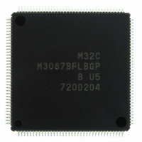
M3087BFLBGP#U5 Renesas Electronics America, M3087BFLBGP#U5 Datasheet - Page 82

M3087BFLBGP#U5
Manufacturer Part Number
M3087BFLBGP#U5
Description
IC M32C/87 MCU FLASH 144LQFP
Manufacturer
Renesas Electronics America
Series
M16C™ M32C/80r
Datasheet
1.M3087BFLGPU3.pdf
(629 pages)
Specifications of M3087BFLBGP#U5
Core Processor
M32C/80
Core Size
16/32-Bit
Speed
32MHz
Connectivity
EBI/EMI, I²C, IEBus, IrDA, SIO, UART/USART
Peripherals
DMA, POR, PWM, WDT
Number Of I /o
121
Program Memory Size
1MB (1M x 8)
Program Memory Type
FLASH
Ram Size
48K x 8
Voltage - Supply (vcc/vdd)
3 V ~ 5.5 V
Data Converters
A/D 34x10b, D/A 2x8b
Oscillator Type
Internal
Operating Temperature
-20°C ~ 85°C
Package / Case
144-LQFP
For Use With
R0K330879S001BE - KIT DEV RSK M32C/87R0K330879S000BE - KIT DEV RSK M32C/87
Lead Free Status / RoHS Status
Lead free / RoHS Compliant
Eeprom Size
-
Available stocks
Company
Part Number
Manufacturer
Quantity
Price
Part Number:
M3087BFLBGP#U5M3087BFLBGP#U3
Manufacturer:
Renesas Electronics America
Quantity:
10 000
- Current page: 82 of 629
- Download datasheet (16Mb)
M32C/87 Group (M32C/87, M32C/87A, M32C/87B)
REJ09B0180-0151 Rev.1.51 Jul 31, 2008
Page 58 of 587
6.3
Figure 6.7
6.2.1
The WDC5 bit in the WDC register determines whether it is a reset process when power-on (cold start) or a reset
process when the RESET signal is input during MCU running (warm start). Default value of the WDC5 bit is 0
(cold start) when power-on, and the bit is set to 1 (warm start) by writing given values to the WDC register. The
WDC5 bit does not become 0 even if the hardware reset 1, hardware reset 2, software reset, or watchdog timer reset
is performed.
Figure 6.7 shows an example of cold start/warm start determination function operation.
WDC5 bit
When all the conditions below are met, the Vdet4 detection interrupt is generated and the MCU exits wait mode
as soon as the WAIT instruction is executed or exits stop mode as soon as the CM10 bit in the CM1 register is
set to 1 (all clocks stopped).
Execute the WAIT instruction or set the CM10 bit to 1 (all clocks stop) while the VC13 bit is 0
(VCC1 < Vdet4), if the MCU is configured to enter wait/stop mode when voltage applied to the VCC1 pin
drops Vdet4 or below and to exit wait/stop mode when the voltage applied rises to Vdet4 or above.
If the Vdet4 detection interrupt has been used to exit wait mode or stop mode, set the D41 bit to 0 and then set it
back to 1 to use the Vdet4 detection interrupt again to exit wait/stop mode.
RESET
VCC1
Cold Start/Warm Start Determination Function
•
•
•
•
the VC27 bit in the VCR2 register is set to 1 (Vdet4 detection function used)
the D40 bit in the D4INT register is set to 1 (Vdet4 detection interrupt enabled)
the D41 bit in the D4INT register is set to 1 (Vdet4 detection interrupt is used to exit wait/stop mode)
the voltage applied to the VCC1 pin is Vdet4 or above (the VC13 bit in the VCR1 register is 1)
Usage Notes on Vdet4 Detection Interrupt
5 V
0 V
5 V
0 V
1
0
NOTE:
Cold Start/Warm Start Determination Function Operation
1. If the time difference between T1 and T2 is greater, it may take longer to set the WDC5 bit to 1.
Reset sequence (Approx.20 μ s@16 MHz)
T1
T2
Pch transistor ON (Approx. 4 V)
CPU comes out of reset
T > 100 μ s
Program starts running
Set to 1 by a program
The WDC5 bit remains set
to 1 even if voltage applied
to RESET becomes 0 V.
6. Power Supply Voltage Detection Function
Related parts for M3087BFLBGP#U5
Image
Part Number
Description
Manufacturer
Datasheet
Request
R

Part Number:
Description:
KIT STARTER FOR M16C/29
Manufacturer:
Renesas Electronics America
Datasheet:

Part Number:
Description:
KIT STARTER FOR R8C/2D
Manufacturer:
Renesas Electronics America
Datasheet:

Part Number:
Description:
R0K33062P STARTER KIT
Manufacturer:
Renesas Electronics America
Datasheet:

Part Number:
Description:
KIT STARTER FOR R8C/23 E8A
Manufacturer:
Renesas Electronics America
Datasheet:

Part Number:
Description:
KIT STARTER FOR R8C/25
Manufacturer:
Renesas Electronics America
Datasheet:

Part Number:
Description:
KIT STARTER H8S2456 SHARPE DSPLY
Manufacturer:
Renesas Electronics America
Datasheet:

Part Number:
Description:
KIT STARTER FOR R8C38C
Manufacturer:
Renesas Electronics America
Datasheet:

Part Number:
Description:
KIT STARTER FOR R8C35C
Manufacturer:
Renesas Electronics America
Datasheet:

Part Number:
Description:
KIT STARTER FOR R8CL3AC+LCD APPS
Manufacturer:
Renesas Electronics America
Datasheet:

Part Number:
Description:
KIT STARTER FOR RX610
Manufacturer:
Renesas Electronics America
Datasheet:

Part Number:
Description:
KIT STARTER FOR R32C/118
Manufacturer:
Renesas Electronics America
Datasheet:

Part Number:
Description:
KIT DEV RSK-R8C/26-29
Manufacturer:
Renesas Electronics America
Datasheet:

Part Number:
Description:
KIT STARTER FOR SH7124
Manufacturer:
Renesas Electronics America
Datasheet:

Part Number:
Description:
KIT STARTER FOR H8SX/1622
Manufacturer:
Renesas Electronics America
Datasheet:

Part Number:
Description:
KIT DEV FOR SH7203
Manufacturer:
Renesas Electronics America
Datasheet:


