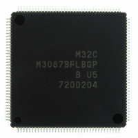
M3087BFLBGP#U5 Renesas Electronics America, M3087BFLBGP#U5 Datasheet - Page 333

M3087BFLBGP#U5
Manufacturer Part Number
M3087BFLBGP#U5
Description
IC M32C/87 MCU FLASH 144LQFP
Manufacturer
Renesas Electronics America
Series
M16C™ M32C/80r
Datasheet
1.M3087BFLGPU3.pdf
(629 pages)
Specifications of M3087BFLBGP#U5
Core Processor
M32C/80
Core Size
16/32-Bit
Speed
32MHz
Connectivity
EBI/EMI, I²C, IEBus, IrDA, SIO, UART/USART
Peripherals
DMA, POR, PWM, WDT
Number Of I /o
121
Program Memory Size
1MB (1M x 8)
Program Memory Type
FLASH
Ram Size
48K x 8
Voltage - Supply (vcc/vdd)
3 V ~ 5.5 V
Data Converters
A/D 34x10b, D/A 2x8b
Oscillator Type
Internal
Operating Temperature
-20°C ~ 85°C
Package / Case
144-LQFP
For Use With
R0K330879S001BE - KIT DEV RSK M32C/87R0K330879S000BE - KIT DEV RSK M32C/87
Lead Free Status / RoHS Status
Lead free / RoHS Compliant
Eeprom Size
-
Available stocks
Company
Part Number
Manufacturer
Quantity
Price
Part Number:
M3087BFLBGP#U5M3087BFLBGP#U3
Manufacturer:
Renesas Electronics America
Quantity:
10 000
- Current page: 333 of 629
- Download datasheet (16Mb)
M32C/87 Group (M32C/87, M32C/87A, M32C/87B)
REJ09B0180-0151 Rev.1.51 Jul 31, 2008
Page 309 of 587
18.2
18.2.1
18.2.2
18.2.3
Table 18.11
NOTES:
18.2.4
18.2.5
AD0CON0 Register
1. A/D conversion starts when the ADST bit is set to 1 (A/D conversion starts) and a trigger is generated.
2. A/D conversion starts over from the beginning, if an external trigger or a hardware trigger is inserted during
The BITS bit in the AD0CON1 register determines the resolution. When the BITS bit is set to 1 (10-bit mode),
the A/D conversion result is stored into bits 9 to 0 in the AD0i register (i = 0 to 7). When the BITS bit is set to 0
(8-bit mode), the A/D conversion result is stored into bits 7 to 0 in the AD0i register.
When the SMP bit in the AD0CON2 register is set to 1 (with sample and hold), the A/D conversion rate per pin
increases to 28 φAD cycles for 8-bit resolution and 33 φAD cycles for 10-bit resolution. The sample and hold
function is available in all operating modes. Start A/D conversion after selecting whether the sample and hold
circuit is used or not.
The TRG bit in the AD0CON0 register and the TRG0 bit in the AD0CON2 register determine a trigger to start
A/D conversion. Table 18.11 lists setting values for the trigger select function.
DMAC operating mode is available in all operating modes. To select multi-port single sweep mode or multi-
port repeat sweep mode 0, DMAC operating mode must be used. When the DUS bit in the AD0CON3 register
is set to 1 (DMAC operating mode used), all A/D conversion results are stored into the AD00 register. DMAC
transfers the result from the AD00 register to a given memory space every time A/D conversion on a single pin
is completed. 8-bit DMA transfer must be selected for 8-bit resolution and 16-bit DMA transfer for 10-bit
resolution. Refer to 13. DMAC for DMAC instructions.
When using DMAC operating mode in single sweep mode, repeat sweep mode 0, repeat sweep mode 1, multi-
port single sweep mode, or multi-port repeat sweep mode 0, do not generate an external retrigger or hardware
retrigger.
In one-shot mode and repeat mode, the ANEX0 pin or ANEX1 pin can be used as the analog input pin. These
pins can be selected using bits OPA1 and OPA0 in the AD0CON1 register. The A/D conversion result for
ANEX0 input is stored into the AD00 register, and for ANEX1 input into the AD01 register. Both results are
stored into the AD00 register when the DUS bit in the AD0CON3 register is set to 1 (DMAC operating mode
used).
Set bits APS1 and APS0 in the AD0CON2 register to 00b (AN_0 to AN_7, ANEX0, ANEX1) and the MSS bit
in the AD0CON3 register to 0 (multi-port sweep mode not used).
TRG = 1
A/D conversion. (A/D conversion in progress is aborted.)
TRG = 0
Functions
Resolution
Sample and Hold
Trigger Select Function
DMAC Operating Mode
Extended Analog Input Pins
(1)
Trigger Select Function Setting Values
Bit and Setting
AD0CON2 Register
TRG0 = 0
TRG0 = 1
−
Software trigger
External trigger
Hardware trigger
A/D conversion starts when the ADST bit in the AD0CON0
register is set to 1 by a program
Falling edge of a signal applied to ADTRG
Timer B2 interrupt request of three-phase motor control timer
function (after the ICTB2 register completes counting)
(2)
(2)
Trigger
18. A/D Converter
Related parts for M3087BFLBGP#U5
Image
Part Number
Description
Manufacturer
Datasheet
Request
R

Part Number:
Description:
KIT STARTER FOR M16C/29
Manufacturer:
Renesas Electronics America
Datasheet:

Part Number:
Description:
KIT STARTER FOR R8C/2D
Manufacturer:
Renesas Electronics America
Datasheet:

Part Number:
Description:
R0K33062P STARTER KIT
Manufacturer:
Renesas Electronics America
Datasheet:

Part Number:
Description:
KIT STARTER FOR R8C/23 E8A
Manufacturer:
Renesas Electronics America
Datasheet:

Part Number:
Description:
KIT STARTER FOR R8C/25
Manufacturer:
Renesas Electronics America
Datasheet:

Part Number:
Description:
KIT STARTER H8S2456 SHARPE DSPLY
Manufacturer:
Renesas Electronics America
Datasheet:

Part Number:
Description:
KIT STARTER FOR R8C38C
Manufacturer:
Renesas Electronics America
Datasheet:

Part Number:
Description:
KIT STARTER FOR R8C35C
Manufacturer:
Renesas Electronics America
Datasheet:

Part Number:
Description:
KIT STARTER FOR R8CL3AC+LCD APPS
Manufacturer:
Renesas Electronics America
Datasheet:

Part Number:
Description:
KIT STARTER FOR RX610
Manufacturer:
Renesas Electronics America
Datasheet:

Part Number:
Description:
KIT STARTER FOR R32C/118
Manufacturer:
Renesas Electronics America
Datasheet:

Part Number:
Description:
KIT DEV RSK-R8C/26-29
Manufacturer:
Renesas Electronics America
Datasheet:

Part Number:
Description:
KIT STARTER FOR SH7124
Manufacturer:
Renesas Electronics America
Datasheet:

Part Number:
Description:
KIT STARTER FOR H8SX/1622
Manufacturer:
Renesas Electronics America
Datasheet:

Part Number:
Description:
KIT DEV FOR SH7203
Manufacturer:
Renesas Electronics America
Datasheet:


