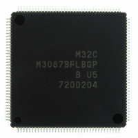
M3087BFLBGP#U5 Renesas Electronics America, M3087BFLBGP#U5 Datasheet - Page 585

M3087BFLBGP#U5
Manufacturer Part Number
M3087BFLBGP#U5
Description
IC M32C/87 MCU FLASH 144LQFP
Manufacturer
Renesas Electronics America
Series
M16C™ M32C/80r
Datasheet
1.M3087BFLGPU3.pdf
(629 pages)
Specifications of M3087BFLBGP#U5
Core Processor
M32C/80
Core Size
16/32-Bit
Speed
32MHz
Connectivity
EBI/EMI, I²C, IEBus, IrDA, SIO, UART/USART
Peripherals
DMA, POR, PWM, WDT
Number Of I /o
121
Program Memory Size
1MB (1M x 8)
Program Memory Type
FLASH
Ram Size
48K x 8
Voltage - Supply (vcc/vdd)
3 V ~ 5.5 V
Data Converters
A/D 34x10b, D/A 2x8b
Oscillator Type
Internal
Operating Temperature
-20°C ~ 85°C
Package / Case
144-LQFP
For Use With
R0K330879S001BE - KIT DEV RSK M32C/87R0K330879S000BE - KIT DEV RSK M32C/87
Lead Free Status / RoHS Status
Lead free / RoHS Compliant
Eeprom Size
-
Available stocks
Company
Part Number
Manufacturer
Quantity
Price
Part Number:
M3087BFLBGP#U5M3087BFLBGP#U3
Manufacturer:
Renesas Electronics America
Quantity:
10 000
- Current page: 585 of 629
- Download datasheet (16Mb)
M32C/87 Group (M32C/87, M32C/87A, M32C/87B)
REJ09B0180-0151 Rev.1.51 Jul 31, 2008
Page 561 of 587
28.5
28.5.1
28.5.2
28.5.3
28.5.4
28.5.2.1
28.5.2.2
28.5.4.1
To oscillate the sub clock, set the CM07 bit in the CM0 register to 0 (clock other than the sub clock) and the
CM03 bit to 1 (XCIN-XOUT drive capability = high). Then, set the CM04 bit in the CM0 register to 1 (XCIN-
XCOUT oscillation function). Once the sub clock becomes stabilized, set the CM03 bit to 0 (XCIN-XOUT
drive capability = low).
After the above procedure, the sub clock can be used as the CPU clock, or the count source for timer A and
timer B.
(Technical update: TN-16C-119A/EA)
If an oscillation circuit constant matching for the sub clock oscillation circuit has only been evaluated with the
drive capability = high, the constant matching for drive capability = low must also be evaluated.
Contact your oscillator manufacturer for details on the oscillation circuit constant matching.
To change bits MCD4 to MCD0, set the PM12 bit in the PM1 register to 0 (no wait state).
Stabilize the main clock, sub clock, or PLL clock prior to switching the clock source for the CPU clock to one
of these clocks.
Clock Generation Circuits
•
•
•
•
•
•
When the CPU operating frequency is required 24 MHz or higher, make an oscillator connected to the main
clock circuit (XIN-XOUT), or a clock applied to the XIN pin have 24 MHz or lower frequency, and then
multiply the main clock with the PLL frequency synthesizer. By using this procedure, a better EMC
(Electromagnetic Compatibility) performance can be achieved than connecting a 24 MHz or higher
frequency oscillator or using 24 MHz or higher input clock applied to the XIN pin.
the external clock.
(Technical update: TN-M16C-109-0309)
When a clock applied to the XIN pin is used for the CPU clock, do not set the CM05 bit in the CM0 register
to 1 (stopped).
When entering wait mode with setting the CM02 bit in the CM0 register to 1 (peripheral clocks stop in wait
mode), set bits MCD4 to MCD0 in the MCD register for CPU clock frequency to be 10-MHz or lower after
dividing the main clock.
When entering wait mode, the instructions following the WAIT instruction are stored into the instruction
queue, and the program stops. Insert at least 4 NOP instructions after the WAIT instruction.
To enter wait mode, execute the WAIT instruction while a high-level (“H”) signal is applied to the NMI
pin.
If the main clock is selected as the CPU clock while an external clock is applied to the XIN pin, do not stop
Main Clock
Sub Clock
Clock Dividing Ratio
Power Consumption Control
To Oscillate Sub Clock
Oscillation Parameter Matching
Wait Mode
28. Usage Notes
Related parts for M3087BFLBGP#U5
Image
Part Number
Description
Manufacturer
Datasheet
Request
R

Part Number:
Description:
KIT STARTER FOR M16C/29
Manufacturer:
Renesas Electronics America
Datasheet:

Part Number:
Description:
KIT STARTER FOR R8C/2D
Manufacturer:
Renesas Electronics America
Datasheet:

Part Number:
Description:
R0K33062P STARTER KIT
Manufacturer:
Renesas Electronics America
Datasheet:

Part Number:
Description:
KIT STARTER FOR R8C/23 E8A
Manufacturer:
Renesas Electronics America
Datasheet:

Part Number:
Description:
KIT STARTER FOR R8C/25
Manufacturer:
Renesas Electronics America
Datasheet:

Part Number:
Description:
KIT STARTER H8S2456 SHARPE DSPLY
Manufacturer:
Renesas Electronics America
Datasheet:

Part Number:
Description:
KIT STARTER FOR R8C38C
Manufacturer:
Renesas Electronics America
Datasheet:

Part Number:
Description:
KIT STARTER FOR R8C35C
Manufacturer:
Renesas Electronics America
Datasheet:

Part Number:
Description:
KIT STARTER FOR R8CL3AC+LCD APPS
Manufacturer:
Renesas Electronics America
Datasheet:

Part Number:
Description:
KIT STARTER FOR RX610
Manufacturer:
Renesas Electronics America
Datasheet:

Part Number:
Description:
KIT STARTER FOR R32C/118
Manufacturer:
Renesas Electronics America
Datasheet:

Part Number:
Description:
KIT DEV RSK-R8C/26-29
Manufacturer:
Renesas Electronics America
Datasheet:

Part Number:
Description:
KIT STARTER FOR SH7124
Manufacturer:
Renesas Electronics America
Datasheet:

Part Number:
Description:
KIT STARTER FOR H8SX/1622
Manufacturer:
Renesas Electronics America
Datasheet:

Part Number:
Description:
KIT DEV FOR SH7203
Manufacturer:
Renesas Electronics America
Datasheet:


