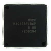
M3087BFLBGP#U5 Renesas Electronics America, M3087BFLBGP#U5 Datasheet - Page 50

M3087BFLBGP#U5
Manufacturer Part Number
M3087BFLBGP#U5
Description
IC M32C/87 MCU FLASH 144LQFP
Manufacturer
Renesas Electronics America
Series
M16C™ M32C/80r
Datasheet
1.M3087BFLGPU3.pdf
(629 pages)
Specifications of M3087BFLBGP#U5
Core Processor
M32C/80
Core Size
16/32-Bit
Speed
32MHz
Connectivity
EBI/EMI, I²C, IEBus, IrDA, SIO, UART/USART
Peripherals
DMA, POR, PWM, WDT
Number Of I /o
121
Program Memory Size
1MB (1M x 8)
Program Memory Type
FLASH
Ram Size
48K x 8
Voltage - Supply (vcc/vdd)
3 V ~ 5.5 V
Data Converters
A/D 34x10b, D/A 2x8b
Oscillator Type
Internal
Operating Temperature
-20°C ~ 85°C
Package / Case
144-LQFP
For Use With
R0K330879S001BE - KIT DEV RSK M32C/87R0K330879S000BE - KIT DEV RSK M32C/87
Lead Free Status / RoHS Status
Lead free / RoHS Compliant
Eeprom Size
-
Available stocks
Company
Part Number
Manufacturer
Quantity
Price
Part Number:
M3087BFLBGP#U5M3087BFLBGP#U3
Manufacturer:
Renesas Electronics America
Quantity:
10 000
- Current page: 50 of 629
- Download datasheet (16Mb)
M32C/87 Group (M32C/87, M32C/87A, M32C/87B)
REJ09B0180-0151 Rev.1.51 Jul 31, 2008
Page 26 of 587
3.
Figure 3.1 shows a memory map of the M32C/87 Group (M32C/87, M32C/87A, M32C/87B).
The M32C/87 Group (M32C/87, M32C/87A, M32C/87B) has 16-Mbyte address space from addresses 000000h to
FFFFFFh.
The internal ROM is allocated in lower addresses, beginning with address FFFFFFh. For example, a 512-Kbyte
internal ROM area is allocated in addresses F80000h to FFFFFFh.
The fixed interrupt vectors are allocated in addresses FFFFDCh to FFFFFFh. They store the starting address of each
interrupt routine. Refer to 11. Interrupts for details.
The internal RAM is allocated higher addresses, beginning with address 000400h. For example, a 48-Kbyte internal
RAM area is allocated in addresses 000400h to 00C3FFh. The internal RAM is used not only for storing data but for
the stacks when subroutines are called or when interrupt requests are acknowledged.
SFRs are allocated in addresses 000000h to 0003FFh. The peripheral function control registers such as for I/O ports,
A/D converters, serial interfaces, timers are allocated here. All blank spaces within SFRs are reserved and cannot be
accessed by users.
The special page vectors are allocated addresses FFFE00h to FFFFDBh. They are used for the JMPS instruction and
JSRS instruction. Refer to the Renesas publication M32C/80 Series Software Manual for details.
Figure 3.1
Memory
NOTES:
Memory Map
1. The space is used as the external space in memory expansion mode and in microprocessor mode. It is reserved in
2. The space is reserved in memory expansion mode. It is used as the external space in microprocessor mode.
3. Additional 4-Kbyte space is provided in the flash memory version to store data. This space is used in single-chip
4. This space is used in single-chip mode and memory expansion mode. It is used as the external space in
5. The watchdog timer interrupt, oscillation stop detection interrupt, and Vdet4 detection interrupt use the same vector.
single-ship mode.
mode and memory expansion mode. It is reserved in microprocessor mode.
microprocessor mode.
1024 Kbytes
768 Kbytes
384 Kbytes
512 Kbytes
24 Kbytes
31 Kbytes
48 Kbytes
Capacity
Capacity
Internal ROM
Internal RAM
XXXXXXh
YYYYYYh
00C3FFh
0063FFh
007FFFh
FA0000h
F80000h
F40000h
F00000h
XXXXXXh
YYYYYYh
FFFFFFh
00FFFFh
00F000h
F00000h
000000h
000400h
External space
Internal ROM
Internal ROM
Internal RAM
(Data space)
Reserved
Reserved
SFR
(2)
(3)
(4)
(1)
FFFFDCh
FFFFFFh
FFFE00h
Undefined instruction
BRK instruction
Address match
Watchdog timer (5)
Special page
vector table
Overflow
Reset
NMI
3. Memory
Related parts for M3087BFLBGP#U5
Image
Part Number
Description
Manufacturer
Datasheet
Request
R

Part Number:
Description:
KIT STARTER FOR M16C/29
Manufacturer:
Renesas Electronics America
Datasheet:

Part Number:
Description:
KIT STARTER FOR R8C/2D
Manufacturer:
Renesas Electronics America
Datasheet:

Part Number:
Description:
R0K33062P STARTER KIT
Manufacturer:
Renesas Electronics America
Datasheet:

Part Number:
Description:
KIT STARTER FOR R8C/23 E8A
Manufacturer:
Renesas Electronics America
Datasheet:

Part Number:
Description:
KIT STARTER FOR R8C/25
Manufacturer:
Renesas Electronics America
Datasheet:

Part Number:
Description:
KIT STARTER H8S2456 SHARPE DSPLY
Manufacturer:
Renesas Electronics America
Datasheet:

Part Number:
Description:
KIT STARTER FOR R8C38C
Manufacturer:
Renesas Electronics America
Datasheet:

Part Number:
Description:
KIT STARTER FOR R8C35C
Manufacturer:
Renesas Electronics America
Datasheet:

Part Number:
Description:
KIT STARTER FOR R8CL3AC+LCD APPS
Manufacturer:
Renesas Electronics America
Datasheet:

Part Number:
Description:
KIT STARTER FOR RX610
Manufacturer:
Renesas Electronics America
Datasheet:

Part Number:
Description:
KIT STARTER FOR R32C/118
Manufacturer:
Renesas Electronics America
Datasheet:

Part Number:
Description:
KIT DEV RSK-R8C/26-29
Manufacturer:
Renesas Electronics America
Datasheet:

Part Number:
Description:
KIT STARTER FOR SH7124
Manufacturer:
Renesas Electronics America
Datasheet:

Part Number:
Description:
KIT STARTER FOR H8SX/1622
Manufacturer:
Renesas Electronics America
Datasheet:

Part Number:
Description:
KIT DEV FOR SH7203
Manufacturer:
Renesas Electronics America
Datasheet:


