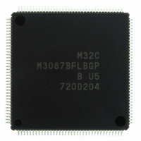
M3087BFLBGP#U5 Renesas Electronics America, M3087BFLBGP#U5 Datasheet - Page 615

M3087BFLBGP#U5
Manufacturer Part Number
M3087BFLBGP#U5
Description
IC M32C/87 MCU FLASH 144LQFP
Manufacturer
Renesas Electronics America
Series
M16C™ M32C/80r
Datasheet
1.M3087BFLGPU3.pdf
(629 pages)
Specifications of M3087BFLBGP#U5
Core Processor
M32C/80
Core Size
16/32-Bit
Speed
32MHz
Connectivity
EBI/EMI, I²C, IEBus, IrDA, SIO, UART/USART
Peripherals
DMA, POR, PWM, WDT
Number Of I /o
121
Program Memory Size
1MB (1M x 8)
Program Memory Type
FLASH
Ram Size
48K x 8
Voltage - Supply (vcc/vdd)
3 V ~ 5.5 V
Data Converters
A/D 34x10b, D/A 2x8b
Oscillator Type
Internal
Operating Temperature
-20°C ~ 85°C
Package / Case
144-LQFP
For Use With
R0K330879S001BE - KIT DEV RSK M32C/87R0K330879S000BE - KIT DEV RSK M32C/87
Lead Free Status / RoHS Status
Lead free / RoHS Compliant
Eeprom Size
-
Available stocks
Company
Part Number
Manufacturer
Quantity
Price
Part Number:
M3087BFLBGP#U5M3087BFLBGP#U3
Manufacturer:
Renesas Electronics America
Quantity:
10 000
- Current page: 615 of 629
- Download datasheet (16Mb)
Rev.
REVISION HISTORY
Date
Page
292
293
295
296
301
303
304
314
330
331
332
333
334
336
339
340
341
343
344
345
346
347
348
355
Intelligent I/O
• Figure 22.5 G1BCR1 Register The RST2 bit function modified, note 2
• Figure 22.6 G2BCR1 Register Note 3 deleted
• Figure 22.8 G1TPR6 and G1TPR7 Registers Note 1 modified
• Figure 22.9 G1POCR0 to G1POCR7 Registers Note 6 and 7 modified
• Table 22.2 Base Timer Specifications Base Timer Reset Condition
• Figure 22.14 Base Timer Block Diagram Diagram modified
• Table 22.3 Base Timer Associated Register Settings Table layout
• Table 22.8 Waveform Generating Function Associated Register
• Figure 22.31 G0RB and G1RB Registers Bit 14 modified as the PER bit
• Figure 22.32 G1MR Register Bit 5 and 4 modified as the PRY and PRYE
• Figure 22.33 G0EMR Register The RXSL and TXSL bit names and
• Figure 22.33 G1EMR Register The RXSL and TXSL bit functions
• Figure 22.34 G0ETC Register Note 1 modified
• Figure 22.34 G1ETC Register Bits 2 to 0 functions modified, note 1
• Figure 22.35 G0ERC and G1ERC Registers Note 1 modified
• Figure 22.37 G1IRF Register Note 1 modified
• Table 22.16 Clock Synchronous Serial I/O Mode Specifications Error
• Table 22.18 Clock Settings in Clock Synchronous Serial I/O Mode
• Table 22.20 Pin Settings in Clock Synchronous Serial I/O Mode
• Table 22.23 Pin Settings Register settings deleted
• Table 22.24 UART Mode Specifications Data Transfer Format, Error
• Table 22.25 Clock Settings in UART Mode “Input form ISCLK1” setting
• Table 22.26 Register Settings in UART Mode The PRY and PRYE bit
• Figure 22.41 Transmit Operation Conditions modified
• Figure 22.42 Receive Operation Conditions modified
• 22.4.3 HDLC Data Processing Mode Description modified
• Table 22.29 HDLC Data Processing Mode Specifications Items
• Table 22.31 Clock Settings in HDLC Processing Mode Setting value of
• Table 22.32 Register Settings in HDLC Processing Mode The G1PO1
• Table 22.35 Pin Settings in Variable Clock Synchronous Serial I/O
modified
modified, Interrupt Request modified
modified
Settings Table layout modified
bits
functions modified
modified
modified
Detection specification modified
Setting value of the G1PO0 register revised
Register settings modified
Detection and Selectable Function specifications modified, note 2
modified
deleted, note 3 modified
functions added
modified, Interrupt Request specifications modified
the G1PO1 register modified
register function modified
Mode The PD7 register settings modified
M32C/87 Group Hardware Manual
C - 4
Description
Summary
Related parts for M3087BFLBGP#U5
Image
Part Number
Description
Manufacturer
Datasheet
Request
R

Part Number:
Description:
KIT STARTER FOR M16C/29
Manufacturer:
Renesas Electronics America
Datasheet:

Part Number:
Description:
KIT STARTER FOR R8C/2D
Manufacturer:
Renesas Electronics America
Datasheet:

Part Number:
Description:
R0K33062P STARTER KIT
Manufacturer:
Renesas Electronics America
Datasheet:

Part Number:
Description:
KIT STARTER FOR R8C/23 E8A
Manufacturer:
Renesas Electronics America
Datasheet:

Part Number:
Description:
KIT STARTER FOR R8C/25
Manufacturer:
Renesas Electronics America
Datasheet:

Part Number:
Description:
KIT STARTER H8S2456 SHARPE DSPLY
Manufacturer:
Renesas Electronics America
Datasheet:

Part Number:
Description:
KIT STARTER FOR R8C38C
Manufacturer:
Renesas Electronics America
Datasheet:

Part Number:
Description:
KIT STARTER FOR R8C35C
Manufacturer:
Renesas Electronics America
Datasheet:

Part Number:
Description:
KIT STARTER FOR R8CL3AC+LCD APPS
Manufacturer:
Renesas Electronics America
Datasheet:

Part Number:
Description:
KIT STARTER FOR RX610
Manufacturer:
Renesas Electronics America
Datasheet:

Part Number:
Description:
KIT STARTER FOR R32C/118
Manufacturer:
Renesas Electronics America
Datasheet:

Part Number:
Description:
KIT DEV RSK-R8C/26-29
Manufacturer:
Renesas Electronics America
Datasheet:

Part Number:
Description:
KIT STARTER FOR SH7124
Manufacturer:
Renesas Electronics America
Datasheet:

Part Number:
Description:
KIT STARTER FOR H8SX/1622
Manufacturer:
Renesas Electronics America
Datasheet:

Part Number:
Description:
KIT DEV FOR SH7203
Manufacturer:
Renesas Electronics America
Datasheet:


