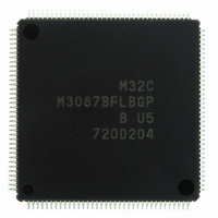
M3087BFLBGP#U5 Renesas Electronics America, M3087BFLBGP#U5 Datasheet - Page 71

M3087BFLBGP#U5
Manufacturer Part Number
M3087BFLBGP#U5
Description
IC M32C/87 MCU FLASH 144LQFP
Manufacturer
Renesas Electronics America
Series
M16C™ M32C/80r
Datasheet
1.M3087BFLGPU3.pdf
(629 pages)
Specifications of M3087BFLBGP#U5
Core Processor
M32C/80
Core Size
16/32-Bit
Speed
32MHz
Connectivity
EBI/EMI, I²C, IEBus, IrDA, SIO, UART/USART
Peripherals
DMA, POR, PWM, WDT
Number Of I /o
121
Program Memory Size
1MB (1M x 8)
Program Memory Type
FLASH
Ram Size
48K x 8
Voltage - Supply (vcc/vdd)
3 V ~ 5.5 V
Data Converters
A/D 34x10b, D/A 2x8b
Oscillator Type
Internal
Operating Temperature
-20°C ~ 85°C
Package / Case
144-LQFP
For Use With
R0K330879S001BE - KIT DEV RSK M32C/87R0K330879S000BE - KIT DEV RSK M32C/87
Lead Free Status / RoHS Status
Lead free / RoHS Compliant
Eeprom Size
-
Available stocks
Company
Part Number
Manufacturer
Quantity
Price
Part Number:
M3087BFLBGP#U5M3087BFLBGP#U3
Manufacturer:
Renesas Electronics America
Quantity:
10 000
- Current page: 71 of 629
- Download datasheet (16Mb)
M32C/87 Group (M32C/87, M32C/87A, M32C/87B)
REJ09B0180-0151 Rev.1.51 Jul 31, 2008
Page 47 of 587
5.
Hardware reset 1, hardware reset 2 (Vdet3 detection function), software reset and watchdog timer reset are
implemented to reset the MCU.
5.1
Figure 5.1
5.1.1
5.1.2
Pins, CPU, and SFRs are reset by using the RESET pin. When a low-level (“L”) signal is applied to the RESET pin
while the supply voltage meets the recommended operating conditions, ports and I/O pins for peripheral functions
are reset. (Refer to Table 5.1 Pin states while RESET pin is held “L”.) Also, the oscillation circuit is reset and the
main clock starts oscillating. CPU and SFRs are reset when the signal applied to the RESET pin changes from “L”
to high-level (“H”) signal, and then the MCU executes a program beginning with the address indicated by the reset
vector. The WDC5 bit in the WDC register and the internal RAM are not reset by hardware reset 1. When an “L”
signal is applied to the RESET pin while writing data to the internal RAM, the value written to the internal RAM
becomes undefined.
Figure 5.1 shows an example of the reset circuit. Figure 5.2 shows a reset sequence. Table 5.1 lists pin states while
the RESET pin is held “L”.
Reset
Hardware Reset 1
(1) Apply an “L” signal to the RESET pin.
(2) Input 20 clock cycles or more into the XIN pin.
(3) Apply an “H” signal to the RESET pin.
(1) Apply an “L” signal to the RESET pin.
(2) Increase the supply voltage until it meets the recommended operating condition.
(3) Wait for td(P-R) (internal power supply stabilization time) or more to allow the internal power supply to
(4) Inputs 20 clock cycles or more into the XIN pin.
(5) Apply an “H” signal to the RESET pin.
NOTE:
1. If operating at VCC1 > VCC2, VCC2 voltage must be lower than VCC1 voltage when powering up and down.
Reset at a Stable Supply Voltage
Power-on Reset
stabilize.
Example of Reset Circuit
VCC1
RESET
RESET
VCC1
0V
0V
operating voltage
Recommended
0.2VCC1 or below
Input td(P-R) + 20 clock cycles or more
to the XIN pin
0.2VCC1 or below
5. Reset
Related parts for M3087BFLBGP#U5
Image
Part Number
Description
Manufacturer
Datasheet
Request
R

Part Number:
Description:
KIT STARTER FOR M16C/29
Manufacturer:
Renesas Electronics America
Datasheet:

Part Number:
Description:
KIT STARTER FOR R8C/2D
Manufacturer:
Renesas Electronics America
Datasheet:

Part Number:
Description:
R0K33062P STARTER KIT
Manufacturer:
Renesas Electronics America
Datasheet:

Part Number:
Description:
KIT STARTER FOR R8C/23 E8A
Manufacturer:
Renesas Electronics America
Datasheet:

Part Number:
Description:
KIT STARTER FOR R8C/25
Manufacturer:
Renesas Electronics America
Datasheet:

Part Number:
Description:
KIT STARTER H8S2456 SHARPE DSPLY
Manufacturer:
Renesas Electronics America
Datasheet:

Part Number:
Description:
KIT STARTER FOR R8C38C
Manufacturer:
Renesas Electronics America
Datasheet:

Part Number:
Description:
KIT STARTER FOR R8C35C
Manufacturer:
Renesas Electronics America
Datasheet:

Part Number:
Description:
KIT STARTER FOR R8CL3AC+LCD APPS
Manufacturer:
Renesas Electronics America
Datasheet:

Part Number:
Description:
KIT STARTER FOR RX610
Manufacturer:
Renesas Electronics America
Datasheet:

Part Number:
Description:
KIT STARTER FOR R32C/118
Manufacturer:
Renesas Electronics America
Datasheet:

Part Number:
Description:
KIT DEV RSK-R8C/26-29
Manufacturer:
Renesas Electronics America
Datasheet:

Part Number:
Description:
KIT STARTER FOR SH7124
Manufacturer:
Renesas Electronics America
Datasheet:

Part Number:
Description:
KIT STARTER FOR H8SX/1622
Manufacturer:
Renesas Electronics America
Datasheet:

Part Number:
Description:
KIT DEV FOR SH7203
Manufacturer:
Renesas Electronics America
Datasheet:


