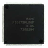
M3087BFLBGP#U5 Renesas Electronics America, M3087BFLBGP#U5 Datasheet - Page 521

M3087BFLBGP#U5
Manufacturer Part Number
M3087BFLBGP#U5
Description
IC M32C/87 MCU FLASH 144LQFP
Manufacturer
Renesas Electronics America
Series
M16C™ M32C/80r
Datasheet
1.M3087BFLGPU3.pdf
(629 pages)
Specifications of M3087BFLBGP#U5
Core Processor
M32C/80
Core Size
16/32-Bit
Speed
32MHz
Connectivity
EBI/EMI, I²C, IEBus, IrDA, SIO, UART/USART
Peripherals
DMA, POR, PWM, WDT
Number Of I /o
121
Program Memory Size
1MB (1M x 8)
Program Memory Type
FLASH
Ram Size
48K x 8
Voltage - Supply (vcc/vdd)
3 V ~ 5.5 V
Data Converters
A/D 34x10b, D/A 2x8b
Oscillator Type
Internal
Operating Temperature
-20°C ~ 85°C
Package / Case
144-LQFP
For Use With
R0K330879S001BE - KIT DEV RSK M32C/87R0K330879S000BE - KIT DEV RSK M32C/87
Lead Free Status / RoHS Status
Lead free / RoHS Compliant
Eeprom Size
-
Available stocks
Company
Part Number
Manufacturer
Quantity
Price
Part Number:
M3087BFLBGP#U5M3087BFLBGP#U3
Manufacturer:
Renesas Electronics America
Quantity:
10 000
- Current page: 521 of 629
- Download datasheet (16Mb)
M32C/87 Group (M32C/87, M32C/87A, M32C/87B)
REJ09B0180-0151 Rev.1.51 Jul 31, 2008
Page 497 of 587
26.3
Table 26.3
NOTES:
Operation
Processor mode
Areas where a rewrite
program can be stored
Software command
Flash memory mode after
erasing or programming
Flash memory status
detection
CPU status during erase
or program operation
Peripheral interrupt
request, DMA request,
and DMACII request
during erase or program
operation
In CPU rewrite mode, the user ROM area can be programmed by the CPU writing software commands with the
MCU mounted on a board. In CPU rewrite mode, only the user ROM area shown in Figure 26.1 can be
programmed. The boot ROM area cannot be rewritten. EW0 mode and EW1 mode are provided as CPU rewrite
mode.
Table 26.3 lists specifications of EW0 mode and EW1 mode. Figures 26.4 and 26.5 show associated registers.
Figure 26.6 shows a setting procedure for EW0 mode. Figure 26.7 shows a setting procedure for EW1 mode.
Figure 26.8 shows a setting procedure to enter and exit low power mode.
1. In both the EW0 mode and EW1 mode, when an NMI interrupt or watchdog timer interrupt is generated, the
2. To use peripheral function interrupts, place interrupt routine programs and the relocatable vector table in an
erase or program operation in progress is aborted and the interrupt is acknowledged.
area other than flash memory.
CPU Rewrite Mode
Item
Specifications of EW0 Mode and EW1 Mode
• Program the user ROM area by executing
• Single-chip mode
• Memory expansion mode
• Boot mode
• User ROM area (Single-chip mode,
• Boot ROM area (Boot mode)
All commands are available.
Read status register mode
• Read bits FMR00, FMR06, and FMR07 in
• Execute the read status register
Operating
Acknowledged
the rewrite control program placed in an
area other than the flash memory.
memory expansion mode)
the FMR0 register by a program.
command to read bits SR7, SR5, and
SR4 in the SRD register.
(2)
EW0 Mode
• Erase and program a block where the
• Single-chip mode
• User ROM area
• All commands, except read status register
Read array mode
• Read bits FMR00, FMR06, and FMR07 in
In a hold state (Stop)
(I/O port maintains the status which is
before executing a command.)
Not acknowledged
(it is acknowledged after completion of
erase or program operation.)
rewrite control program is not placed, by
executing the rewrite control program
placed in the user ROM area.
command, are available.
the FMR0 register by a program.
EW1 Mode
26. Flash Memory
Related parts for M3087BFLBGP#U5
Image
Part Number
Description
Manufacturer
Datasheet
Request
R

Part Number:
Description:
KIT STARTER FOR M16C/29
Manufacturer:
Renesas Electronics America
Datasheet:

Part Number:
Description:
KIT STARTER FOR R8C/2D
Manufacturer:
Renesas Electronics America
Datasheet:

Part Number:
Description:
R0K33062P STARTER KIT
Manufacturer:
Renesas Electronics America
Datasheet:

Part Number:
Description:
KIT STARTER FOR R8C/23 E8A
Manufacturer:
Renesas Electronics America
Datasheet:

Part Number:
Description:
KIT STARTER FOR R8C/25
Manufacturer:
Renesas Electronics America
Datasheet:

Part Number:
Description:
KIT STARTER H8S2456 SHARPE DSPLY
Manufacturer:
Renesas Electronics America
Datasheet:

Part Number:
Description:
KIT STARTER FOR R8C38C
Manufacturer:
Renesas Electronics America
Datasheet:

Part Number:
Description:
KIT STARTER FOR R8C35C
Manufacturer:
Renesas Electronics America
Datasheet:

Part Number:
Description:
KIT STARTER FOR R8CL3AC+LCD APPS
Manufacturer:
Renesas Electronics America
Datasheet:

Part Number:
Description:
KIT STARTER FOR RX610
Manufacturer:
Renesas Electronics America
Datasheet:

Part Number:
Description:
KIT STARTER FOR R32C/118
Manufacturer:
Renesas Electronics America
Datasheet:

Part Number:
Description:
KIT DEV RSK-R8C/26-29
Manufacturer:
Renesas Electronics America
Datasheet:

Part Number:
Description:
KIT STARTER FOR SH7124
Manufacturer:
Renesas Electronics America
Datasheet:

Part Number:
Description:
KIT STARTER FOR H8SX/1622
Manufacturer:
Renesas Electronics America
Datasheet:

Part Number:
Description:
KIT DEV FOR SH7203
Manufacturer:
Renesas Electronics America
Datasheet:


