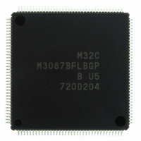
M3087BFLBGP#U5 Renesas Electronics America, M3087BFLBGP#U5 Datasheet - Page 384

M3087BFLBGP#U5
Manufacturer Part Number
M3087BFLBGP#U5
Description
IC M32C/87 MCU FLASH 144LQFP
Manufacturer
Renesas Electronics America
Series
M16C™ M32C/80r
Datasheet
1.M3087BFLGPU3.pdf
(629 pages)
Specifications of M3087BFLBGP#U5
Core Processor
M32C/80
Core Size
16/32-Bit
Speed
32MHz
Connectivity
EBI/EMI, I²C, IEBus, IrDA, SIO, UART/USART
Peripherals
DMA, POR, PWM, WDT
Number Of I /o
121
Program Memory Size
1MB (1M x 8)
Program Memory Type
FLASH
Ram Size
48K x 8
Voltage - Supply (vcc/vdd)
3 V ~ 5.5 V
Data Converters
A/D 34x10b, D/A 2x8b
Oscillator Type
Internal
Operating Temperature
-20°C ~ 85°C
Package / Case
144-LQFP
For Use With
R0K330879S001BE - KIT DEV RSK M32C/87R0K330879S000BE - KIT DEV RSK M32C/87
Lead Free Status / RoHS Status
Lead free / RoHS Compliant
Eeprom Size
-
Available stocks
Company
Part Number
Manufacturer
Quantity
Price
Part Number:
M3087BFLBGP#U5M3087BFLBGP#U3
Manufacturer:
Renesas Electronics America
Quantity:
10 000
- Current page: 384 of 629
- Download datasheet (16Mb)
M32C/87 Group (M32C/87, M32C/87A, M32C/87B)
REJ09B0180-0151 Rev.1.51 Jul 31, 2008
Page 360 of 587
22.3.4
Table 22.10
NOTES:
Waveform generation channels
OUTC2_i pin
Output waveform
Waveform output start condition
Waveform output stop condition
Interrupt request generation timing An interrupt request is generated at the second clock cycle after the base timer
Selectable function
1. Channels 0 to 7 are provided in the 144-pin package. Channels 0 to 2 are provided in the 100-pin package.
2. Set bits RST2 to RST0 in the G2BCR1 register to 000b to use bit modulation PWM mode.
3. When the INV bit in the G2POCRi register is set to 1 (output inverted), the “L” width and the “H” width are
In bit modulation PWM output mode, 16-bit PWM duty ratio can be achieved with a collection of 6-bit PWM
pulses. A series of 1024 pulses whose “L” widths are specified with 6-bit PWM, is repeatedly output. The six
high-order bits in the G2POi register (i = 0 to 7) determine the base “L” width. The ten low-order bits determine
the number of pulses (modulated pulses) whose “L” widths are extended by one fBT2 clock cycle.
Table 22.10 lists specifications of bit modulation PWM output mode. Table 22.11 lists the number of modulated
pulses and their locations. Figure 22.30 shows an example of bit modulation PWM output mode operation.
inversed.
Bit Modulation PWM Output Mode (Group 2)
Item
Specifications of Bit Modulation PWM Output Mode
(2)(3)
Group 2: channels 0 to 7
Pulse output
PWM cycle:
Repeat cycle:
“L” width:
Average “L” width:
n: setting value of the six high-order bits in the G2POi register (00h to 3Fh)
m: setting value of the ten low-order bits in the G2POi register (000h to 3FFh)
Set both the BTS bit in the G2BCR1 register and the IFEi bit in the G2FE register
to 1
Set either the BTS or IFEi bit to 0
value matches the G2POi register value.
• Initial value set function:
• Inverted output function:
The PO2iR bit in the IIOkIR register (k = 3, 5 to 11) becomes 1 (interrupt
requested) when an interrupt request is generated.
(See Figure 11.18 IIO0IR to IIO11IR Registers)
Set the initial output level when waveform output is started (determined by the
IVL bit in the G2POCRi register)
Output the inverted waveform level (determined by the INV bit in the G2POCRi
register)
65536
fBT2
fBT2
fBT2
fBT2
n+1
64
1
(1)
22. Intelligent I/O (Waveform Generation Function)
( = t )
( =
: for m pulses,
× ( n +
fBT2
Specification
64
× 1024 )
1024
m
)
fBT2
n
: for (1024 - m) pulses
Related parts for M3087BFLBGP#U5
Image
Part Number
Description
Manufacturer
Datasheet
Request
R

Part Number:
Description:
KIT STARTER FOR M16C/29
Manufacturer:
Renesas Electronics America
Datasheet:

Part Number:
Description:
KIT STARTER FOR R8C/2D
Manufacturer:
Renesas Electronics America
Datasheet:

Part Number:
Description:
R0K33062P STARTER KIT
Manufacturer:
Renesas Electronics America
Datasheet:

Part Number:
Description:
KIT STARTER FOR R8C/23 E8A
Manufacturer:
Renesas Electronics America
Datasheet:

Part Number:
Description:
KIT STARTER FOR R8C/25
Manufacturer:
Renesas Electronics America
Datasheet:

Part Number:
Description:
KIT STARTER H8S2456 SHARPE DSPLY
Manufacturer:
Renesas Electronics America
Datasheet:

Part Number:
Description:
KIT STARTER FOR R8C38C
Manufacturer:
Renesas Electronics America
Datasheet:

Part Number:
Description:
KIT STARTER FOR R8C35C
Manufacturer:
Renesas Electronics America
Datasheet:

Part Number:
Description:
KIT STARTER FOR R8CL3AC+LCD APPS
Manufacturer:
Renesas Electronics America
Datasheet:

Part Number:
Description:
KIT STARTER FOR RX610
Manufacturer:
Renesas Electronics America
Datasheet:

Part Number:
Description:
KIT STARTER FOR R32C/118
Manufacturer:
Renesas Electronics America
Datasheet:

Part Number:
Description:
KIT DEV RSK-R8C/26-29
Manufacturer:
Renesas Electronics America
Datasheet:

Part Number:
Description:
KIT STARTER FOR SH7124
Manufacturer:
Renesas Electronics America
Datasheet:

Part Number:
Description:
KIT STARTER FOR H8SX/1622
Manufacturer:
Renesas Electronics America
Datasheet:

Part Number:
Description:
KIT DEV FOR SH7203
Manufacturer:
Renesas Electronics America
Datasheet:


