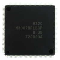
M3087BFLBGP#U5 Renesas Electronics America, M3087BFLBGP#U5 Datasheet - Page 613

M3087BFLBGP#U5
Manufacturer Part Number
M3087BFLBGP#U5
Description
IC M32C/87 MCU FLASH 144LQFP
Manufacturer
Renesas Electronics America
Series
M16C™ M32C/80r
Datasheet
1.M3087BFLGPU3.pdf
(629 pages)
Specifications of M3087BFLBGP#U5
Core Processor
M32C/80
Core Size
16/32-Bit
Speed
32MHz
Connectivity
EBI/EMI, I²C, IEBus, IrDA, SIO, UART/USART
Peripherals
DMA, POR, PWM, WDT
Number Of I /o
121
Program Memory Size
1MB (1M x 8)
Program Memory Type
FLASH
Ram Size
48K x 8
Voltage - Supply (vcc/vdd)
3 V ~ 5.5 V
Data Converters
A/D 34x10b, D/A 2x8b
Oscillator Type
Internal
Operating Temperature
-20°C ~ 85°C
Package / Case
144-LQFP
For Use With
R0K330879S001BE - KIT DEV RSK M32C/87R0K330879S000BE - KIT DEV RSK M32C/87
Lead Free Status / RoHS Status
Lead free / RoHS Compliant
Eeprom Size
-
Available stocks
Company
Part Number
Manufacturer
Quantity
Price
Part Number:
M3087BFLBGP#U5M3087BFLBGP#U3
Manufacturer:
Renesas Electronics America
Quantity:
10 000
- Current page: 613 of 629
- Download datasheet (16Mb)
Rev.
REVISION HISTORY
Date
Page
102
103
111
114
116
120
125
126
127
128
132
136
137
147
153
154
155
160
178
187
59
61
65
84
86
88
89
90
91
94
95
97
99
Processor Mode
• Section structure and description modified
• Figure 6.3 Memory Map in Each Processor Mode Note 3 modified
Bus
• Table 8.3 Processor Mode and Port Function Note 3 modified
Clock Generation Circuit
• Figure 9.4 MCD Register Note 4 added
• Figure 9.6 TCSPR Register Note 2 added
• Figure 9.8 PM2 Register The PM24 and PM25 bit functions modified
• Figure 9.9 Main Clock Circuit Connection Diagram modified
• Figure 9.10 Sub Clock Circuit Connection Diagram modified
• Table 9.2 Bit Settings for On-Chip Oscillator Start Condition added
• Table 9.4 CPU Clock Source and Bit Settings Table modified, note 1
• 9.3.4 fCAN added
• 9.5.2 Wait Mode Structure and description modified
• 9.5.3 Stop Mode Structure and description modified
• Figure 9.13 Status Transition in Wait Mode and Stop Mode Diagram
• Figure 9.14 Status Transition Note 5 added
Interrupt
• Table 11.2 Relocatable Vector Table “Fault error” as interrupt source
• Figure 11.3 Interrupt Control register (1) Note 3 modified
• Figure 11.5 RLVL Register Value after reset modified, note 3 modified,
• 11.6.6 Saving a Register Description modified
• Figure 11.12 Key Input Interrupt Diagram modified
• Figure 11.13 AIER Register Value after reset revised
• Figure 11.14 Intelligent I/O Interrupt and CAN Interrupt Notes 1 and 2
• Description revised, note 1 added
Watchdog Timer
• Figure 12.2 WDC Register Note 3 added
DMAC
• Table 13.1 DMAC Specifications DMA Transfer Cycle specification
• Figure 13.2 DM0SL to DM3SL Registers Value after reset modified
DMAC II
• Figure 14.1 RLVL Register Value after reset modified, note 3 modified,
• Figure 14.5 Transfer Cycle Values in the diagram modified
Timer
• Figure 15.1 Timer A Configuration Diagram modified
• Figure 15.2 Timer B Configuration Diagram modified
• Figure 15.7 TCSPR Register Note 2 added
• Figure 15.21 TB0MR to TB5MR Registers The TCK1 bit function modified
Three-Phase Motor Control Timer Functions
• Figure 16.4 IDB0 and IDB1 Registers Value after reset modified
added
modified, note 2 deleted
deleted, note 4 deleted, note 5 added
note 4 added
revised
modified, note 2 added
note 4 added
M32C/87 Group Hardware Manual
C - 2
Description
Summary
Related parts for M3087BFLBGP#U5
Image
Part Number
Description
Manufacturer
Datasheet
Request
R

Part Number:
Description:
KIT STARTER FOR M16C/29
Manufacturer:
Renesas Electronics America
Datasheet:

Part Number:
Description:
KIT STARTER FOR R8C/2D
Manufacturer:
Renesas Electronics America
Datasheet:

Part Number:
Description:
R0K33062P STARTER KIT
Manufacturer:
Renesas Electronics America
Datasheet:

Part Number:
Description:
KIT STARTER FOR R8C/23 E8A
Manufacturer:
Renesas Electronics America
Datasheet:

Part Number:
Description:
KIT STARTER FOR R8C/25
Manufacturer:
Renesas Electronics America
Datasheet:

Part Number:
Description:
KIT STARTER H8S2456 SHARPE DSPLY
Manufacturer:
Renesas Electronics America
Datasheet:

Part Number:
Description:
KIT STARTER FOR R8C38C
Manufacturer:
Renesas Electronics America
Datasheet:

Part Number:
Description:
KIT STARTER FOR R8C35C
Manufacturer:
Renesas Electronics America
Datasheet:

Part Number:
Description:
KIT STARTER FOR R8CL3AC+LCD APPS
Manufacturer:
Renesas Electronics America
Datasheet:

Part Number:
Description:
KIT STARTER FOR RX610
Manufacturer:
Renesas Electronics America
Datasheet:

Part Number:
Description:
KIT STARTER FOR R32C/118
Manufacturer:
Renesas Electronics America
Datasheet:

Part Number:
Description:
KIT DEV RSK-R8C/26-29
Manufacturer:
Renesas Electronics America
Datasheet:

Part Number:
Description:
KIT STARTER FOR SH7124
Manufacturer:
Renesas Electronics America
Datasheet:

Part Number:
Description:
KIT STARTER FOR H8SX/1622
Manufacturer:
Renesas Electronics America
Datasheet:

Part Number:
Description:
KIT DEV FOR SH7203
Manufacturer:
Renesas Electronics America
Datasheet:


