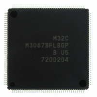
M3087BFLBGP#U5 Renesas Electronics America, M3087BFLBGP#U5 Datasheet - Page 185

M3087BFLBGP#U5
Manufacturer Part Number
M3087BFLBGP#U5
Description
IC M32C/87 MCU FLASH 144LQFP
Manufacturer
Renesas Electronics America
Series
M16C™ M32C/80r
Datasheet
1.M3087BFLGPU3.pdf
(629 pages)
Specifications of M3087BFLBGP#U5
Core Processor
M32C/80
Core Size
16/32-Bit
Speed
32MHz
Connectivity
EBI/EMI, I²C, IEBus, IrDA, SIO, UART/USART
Peripherals
DMA, POR, PWM, WDT
Number Of I /o
121
Program Memory Size
1MB (1M x 8)
Program Memory Type
FLASH
Ram Size
48K x 8
Voltage - Supply (vcc/vdd)
3 V ~ 5.5 V
Data Converters
A/D 34x10b, D/A 2x8b
Oscillator Type
Internal
Operating Temperature
-20°C ~ 85°C
Package / Case
144-LQFP
For Use With
R0K330879S001BE - KIT DEV RSK M32C/87R0K330879S000BE - KIT DEV RSK M32C/87
Lead Free Status / RoHS Status
Lead free / RoHS Compliant
Eeprom Size
-
Available stocks
Company
Part Number
Manufacturer
Quantity
Price
Part Number:
M3087BFLBGP#U5M3087BFLBGP#U3
Manufacturer:
Renesas Electronics America
Quantity:
10 000
- Current page: 185 of 629
- Download datasheet (16Mb)
M32C/87 Group (M32C/87, M32C/87A, M32C/87B)
REJ09B0180-0151 Rev.1.51 Jul 31, 2008
Page 161 of 587
15.1
Figure 15.3
Timer A contains the following four modes. Except in event counter mode, all timers A0 to A4 have the same
functionality. Bits TMOD1 and TMOD0 in the TAiMR register (i = 0 to 4) determine which mode is used.
Figure 15.3 shows a block diagram of timer A. Figures 15.4 to 15.13 show the registers associated with timer A.
Table 15.1 lists TAiOUT pin settings to use in output mode. Table 15.2 lists TAiIN and TAiOUT pin settings to use
in input mode.
TAiIN
TAiOUT
•
•
•
•
Clock source select
Timer mode: The timer counts the internal count source.
Event counter mode: The timer counts overflow/underflow signal of another timer or the external pulses.
One-shot timer mode: The timer operates only once for one trigger.
Pulse width modulation mode: The timer continuously outputs given pulse widths.
i = 0 to 4
j = i - 1, except j = 4 if i = 0
k = i + 1, except k = 0 if i = 4
NOTES:
TCK1 and TCK0, TMOD1 and TMOC0, MR2 and MR1: Bits in the TAiMR register
TAiTGH to TAiTGL: Bits in the ONSF register if i = 0 or bits in the TRGSR register if i = 1 to 4
TAiS: Bit in the TABSR register
TAiUD: Bit in the UDF register
fC32
f2n
f1
f8
Timer A
1. Bits CNT3 to CNT0 in the TCSPR register select no division (n = 0) or
2. Overflow signal or underflow signal.
(1)
Selector
Polarity
divide-by-2n (n = 1 to 15).
00
01
10
11
TCK1 and TCK0
TB2 Overflow
TAk Overflow
TAj Overflow
Timer A Block Diagram
Function select register
(2)
(2)
(2)
00
01
10
11
TAiTGH to TAiTGL
11
· Timer mode
· One-shot timer mode
· Pulse width modulation mode
· Timer Mode (Gate Function)
· Event counter mode
Clock select
Toggle flip flop
TAiUD
TMOD1 and TMOD0, MR2
Decrement
0
1
TAiS
MR2
TAi
Timer A0
Timer A1
Timer A2
Timer A3
Timer A4
00
10
11
01
TMOD1 and TMOD0
0347h 0346h
0349h 0348h
034Bh 034Ah
034Dh 034Ch
034Fh 034Eh
Addresses
High-order bits of data bus
Low-order bits of data bus
Reload register
Increment/decrement
8 low-order
bits
Counter
Always decrement except
in event counter mode
Timer A4
Timer A0
Timer A1
Timer A2
Timer A3
TAj
TAk
Timer A1
Timer A2
Timer A3
Timer A4
Timer A0
8 high-order
bits
15. Timer A
Related parts for M3087BFLBGP#U5
Image
Part Number
Description
Manufacturer
Datasheet
Request
R

Part Number:
Description:
KIT STARTER FOR M16C/29
Manufacturer:
Renesas Electronics America
Datasheet:

Part Number:
Description:
KIT STARTER FOR R8C/2D
Manufacturer:
Renesas Electronics America
Datasheet:

Part Number:
Description:
R0K33062P STARTER KIT
Manufacturer:
Renesas Electronics America
Datasheet:

Part Number:
Description:
KIT STARTER FOR R8C/23 E8A
Manufacturer:
Renesas Electronics America
Datasheet:

Part Number:
Description:
KIT STARTER FOR R8C/25
Manufacturer:
Renesas Electronics America
Datasheet:

Part Number:
Description:
KIT STARTER H8S2456 SHARPE DSPLY
Manufacturer:
Renesas Electronics America
Datasheet:

Part Number:
Description:
KIT STARTER FOR R8C38C
Manufacturer:
Renesas Electronics America
Datasheet:

Part Number:
Description:
KIT STARTER FOR R8C35C
Manufacturer:
Renesas Electronics America
Datasheet:

Part Number:
Description:
KIT STARTER FOR R8CL3AC+LCD APPS
Manufacturer:
Renesas Electronics America
Datasheet:

Part Number:
Description:
KIT STARTER FOR RX610
Manufacturer:
Renesas Electronics America
Datasheet:

Part Number:
Description:
KIT STARTER FOR R32C/118
Manufacturer:
Renesas Electronics America
Datasheet:

Part Number:
Description:
KIT DEV RSK-R8C/26-29
Manufacturer:
Renesas Electronics America
Datasheet:

Part Number:
Description:
KIT STARTER FOR SH7124
Manufacturer:
Renesas Electronics America
Datasheet:

Part Number:
Description:
KIT STARTER FOR H8SX/1622
Manufacturer:
Renesas Electronics America
Datasheet:

Part Number:
Description:
KIT DEV FOR SH7203
Manufacturer:
Renesas Electronics America
Datasheet:


