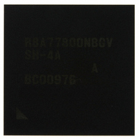
R8A77800ANBGAV Renesas Electronics America, R8A77800ANBGAV Datasheet - Page 1070

R8A77800ANBGAV
Manufacturer Part Number
R8A77800ANBGAV
Description
IC SUPERH MPU ROMLESS 449-BGA
Manufacturer
Renesas Electronics America
Series
SuperH® SH7780r
Datasheet
1.R8A77800ANBGV.pdf
(1342 pages)
Specifications of R8A77800ANBGAV
Core Processor
SH-4A
Core Size
32-Bit
Speed
400MHz
Connectivity
Audio Codec, MMC, Serial Sound, SCI, SIO, SPI, SSI
Peripherals
DMA, POR, WDT
Number Of I /o
75
Program Memory Type
ROMless
Ram Size
16K x 8
Voltage - Supply (vcc/vdd)
1.15 V ~ 1.35 V
Oscillator Type
External
Operating Temperature
-20°C ~ 75°C
Package / Case
449-BGA
Lead Free Status / RoHS Status
Lead free / RoHS Compliant
Eeprom Size
-
Program Memory Size
-
Data Converters
-
Available stocks
Company
Part Number
Manufacturer
Quantity
Price
Company:
Part Number:
R8A77800ANBGAV
Manufacturer:
Renesas Electronics America
Quantity:
10 000
- Current page: 1070 of 1342
- Download datasheet (7Mb)
Section 26 Serial Sound Interface (SSI) Module
When an underflow or overflow error condition is met, the CHNO[1:0] and SWNO bits can be
used to recover the SSI module to a known status. When an underflow or overflow occurs, the
host CPU can read the number of channels and the number of system words to determine what
point the serial audio stream has reached. In the transmitter case, the host CPU can skip forward
through the data it wants to transmit until it finds the sample data that matches what the SSI
module is expecting to transmit next, and so resynchronize with the audio data stream. In the
receiver case, the host CPU can skip forward storing null sample data until it is ready to store the
sample data that the SSI module is indicating that it will receive next to ensure consistency of the
number of received data, and so resynchronize with the audio data stream.
26.4.7
Serial Clock Control
This function is used to control and select which clock is used for the serial bus interface.
If the serial clock direction is set to input (SCKD = 0), the SSI module is in clock slave mode, then
the bit clock that is used in the shift register is derived from the SSI_SCK pin.
If the serial clock direction is set to output (SCKD = 1), the SSI Module is in clock master mode,
and the shift register uses the bit clock derived from the HAC_BIT_CLK input pin or its clock
divided. This input clock is then divided by the ratio in the serial oversampling clock division ratio
(CKDV) bit in SSICR and used as the bit clock in the shift register.
In either case, the SSI_SCK pin output is the same as the bit clock.
Rev.1.00 Dec. 13, 2005 Page 1018 of 1286
REJ09B0158-0100
Related parts for R8A77800ANBGAV
Image
Part Number
Description
Manufacturer
Datasheet
Request
R

Part Number:
Description:
KIT STARTER FOR M16C/29
Manufacturer:
Renesas Electronics America
Datasheet:

Part Number:
Description:
KIT STARTER FOR R8C/2D
Manufacturer:
Renesas Electronics America
Datasheet:

Part Number:
Description:
R0K33062P STARTER KIT
Manufacturer:
Renesas Electronics America
Datasheet:

Part Number:
Description:
KIT STARTER FOR R8C/23 E8A
Manufacturer:
Renesas Electronics America
Datasheet:

Part Number:
Description:
KIT STARTER FOR R8C/25
Manufacturer:
Renesas Electronics America
Datasheet:

Part Number:
Description:
KIT STARTER H8S2456 SHARPE DSPLY
Manufacturer:
Renesas Electronics America
Datasheet:

Part Number:
Description:
KIT STARTER FOR R8C38C
Manufacturer:
Renesas Electronics America
Datasheet:

Part Number:
Description:
KIT STARTER FOR R8C35C
Manufacturer:
Renesas Electronics America
Datasheet:

Part Number:
Description:
KIT STARTER FOR R8CL3AC+LCD APPS
Manufacturer:
Renesas Electronics America
Datasheet:

Part Number:
Description:
KIT STARTER FOR RX610
Manufacturer:
Renesas Electronics America
Datasheet:

Part Number:
Description:
KIT STARTER FOR R32C/118
Manufacturer:
Renesas Electronics America
Datasheet:

Part Number:
Description:
KIT DEV RSK-R8C/26-29
Manufacturer:
Renesas Electronics America
Datasheet:

Part Number:
Description:
KIT STARTER FOR SH7124
Manufacturer:
Renesas Electronics America
Datasheet:

Part Number:
Description:
KIT STARTER FOR H8SX/1622
Manufacturer:
Renesas Electronics America
Datasheet:

Part Number:
Description:
KIT DEV FOR SH7203
Manufacturer:
Renesas Electronics America
Datasheet:


