R8A77800ANBGAV Renesas Electronics America, R8A77800ANBGAV Datasheet - Page 17
R8A77800ANBGAV
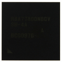
Manufacturer Part Number
R8A77800ANBGAV
Description
IC SUPERH MPU ROMLESS 449-BGA
Manufacturer
Renesas Electronics America
Series
SuperH® SH7780r
Datasheet
1.R8A77800ANBGV.pdf
(1342 pages)
Specifications of R8A77800ANBGAV
Core Processor
SH-4A
Core Size
32-Bit
Speed
400MHz
Connectivity
Audio Codec, MMC, Serial Sound, SCI, SIO, SPI, SSI
Peripherals
DMA, POR, WDT
Number Of I /o
75
Program Memory Type
ROMless
Ram Size
16K x 8
Voltage - Supply (vcc/vdd)
1.15 V ~ 1.35 V
Oscillator Type
External
Operating Temperature
-20°C ~ 75°C
Package / Case
449-BGA
Lead Free Status / RoHS Status
Lead free / RoHS Compliant
Eeprom Size
-
Program Memory Size
-
Data Converters
-
Available stocks
Company
Part Number
Manufacturer
Quantity
Price
Company:

Part Number:
R8A77800ANBGAV
Manufacturer:
Renesas Electronics America
Quantity:
10 000


Section 12 DDR-SDRAM Interface (DDRIF)...................................................401
12.1 Features.............................................................................................................................. 401
12.2 Input/Output Pins ............................................................................................................... 403
12.3 Address Space, Bus Width, and Data Alignment............................................................... 404
12.4 Register Descriptions ......................................................................................................... 410
12.5 Operation ........................................................................................................................... 425
12.6 DDR-SDRAM Basic Timing ............................................................................................. 430
12.7 Usage Notes ....................................................................................................................... 440
Section 13 PCI Controller (PCIC) .....................................................................443
13.1 Features.............................................................................................................................. 443
13.2 Input/Output Pins ............................................................................................................... 446
13.3 Register Descriptions ......................................................................................................... 449
13.4 Operation ........................................................................................................................... 522
12.3.1 Address Space of the DDRIF................................................................................ 404
12.3.2 Memory Data Bus Width ...................................................................................... 405
12.3.3 Data Alignment..................................................................................................... 406
12.4.1 Memory Interface Mode Register (MIM) ............................................................. 412
12.4.2 SDRAM Control Register (SCR).......................................................................... 416
12.4.3 SDRAM Timing Register (STR) .......................................................................... 418
12.4.4 SDRAM Row Attribute Register (SDR)............................................................... 421
12.4.5 SDRAM Mode Register (SDMR)......................................................................... 422
12.4.6 DDR-SDRAM Back-up Register (DBK).............................................................. 424
12.5.1 DDR-SDRAM Access .......................................................................................... 425
12.5.2 DDR-SDRAM Initialization Sequence................................................................. 425
12.5.3 Supported SDRAM Commands............................................................................ 426
12.5.4 SDRAM Access Mode.......................................................................................... 427
12.5.5 Power-Down Modes ............................................................................................. 427
12.5.6 Address Multiplexing ........................................................................................... 429
12.7.1 Operating Frequency............................................................................................. 440
12.7.2 Stopping Clock ..................................................................................................... 440
12.7.3 Using SCR to Issue REFA Command (Outside the Initialization Sequence) ....... 440
12.7.4 Timing of Connected SDRAM ............................................................................. 440
12.7.5 Setting Auto-Refresh Interval ............................................................................... 441
13.3.1 PCIC Enable Control Register (PCIECR) ............................................................ 455
13.3.2 Configuration Registers ........................................................................................ 456
13.3.3 Local Register ....................................................................................................... 481
13.4.1 Supported PCI Commands.................................................................................... 522
13.4.2 PCIC Initialization ................................................................................................ 523
13.4.3 Master Access ....................................................................................................... 524
Rev.1.00 Dec. 13, 2005 Page xv of l
Related parts for R8A77800ANBGAV
Image
Part Number
Description
Manufacturer
Datasheet
Request
R

Part Number:
Description:
KIT STARTER FOR M16C/29
Manufacturer:
Renesas Electronics America
Datasheet:

Part Number:
Description:
KIT STARTER FOR R8C/2D
Manufacturer:
Renesas Electronics America
Datasheet:

Part Number:
Description:
R0K33062P STARTER KIT
Manufacturer:
Renesas Electronics America
Datasheet:

Part Number:
Description:
KIT STARTER FOR R8C/23 E8A
Manufacturer:
Renesas Electronics America
Datasheet:

Part Number:
Description:
KIT STARTER FOR R8C/25
Manufacturer:
Renesas Electronics America
Datasheet:

Part Number:
Description:
KIT STARTER H8S2456 SHARPE DSPLY
Manufacturer:
Renesas Electronics America
Datasheet:

Part Number:
Description:
KIT STARTER FOR R8C38C
Manufacturer:
Renesas Electronics America
Datasheet:

Part Number:
Description:
KIT STARTER FOR R8C35C
Manufacturer:
Renesas Electronics America
Datasheet:

Part Number:
Description:
KIT STARTER FOR R8CL3AC+LCD APPS
Manufacturer:
Renesas Electronics America
Datasheet:
Part Number:
Description:
KIT STARTER FOR RX610
Manufacturer:
Renesas Electronics America
Datasheet:

Part Number:
Description:
KIT STARTER FOR R32C/118
Manufacturer:
Renesas Electronics America
Datasheet:

Part Number:
Description:
KIT DEV RSK-R8C/26-29
Manufacturer:
Renesas Electronics America
Datasheet:

Part Number:
Description:
KIT STARTER FOR SH7124
Manufacturer:
Renesas Electronics America
Datasheet:

Part Number:
Description:
KIT STARTER FOR H8SX/1622
Manufacturer:
Renesas Electronics America
Datasheet:

Part Number:
Description:
KIT DEV FOR SH7203
Manufacturer:
Renesas Electronics America
Datasheet: