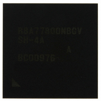
R8A77800ANBGAV Renesas Electronics America, R8A77800ANBGAV Datasheet - Page 290

R8A77800ANBGAV
Manufacturer Part Number
R8A77800ANBGAV
Description
IC SUPERH MPU ROMLESS 449-BGA
Manufacturer
Renesas Electronics America
Series
SuperH® SH7780r
Datasheet
1.R8A77800ANBGV.pdf
(1342 pages)
Specifications of R8A77800ANBGAV
Core Processor
SH-4A
Core Size
32-Bit
Speed
400MHz
Connectivity
Audio Codec, MMC, Serial Sound, SCI, SIO, SPI, SSI
Peripherals
DMA, POR, WDT
Number Of I /o
75
Program Memory Type
ROMless
Ram Size
16K x 8
Voltage - Supply (vcc/vdd)
1.15 V ~ 1.35 V
Oscillator Type
External
Operating Temperature
-20°C ~ 75°C
Package / Case
449-BGA
Lead Free Status / RoHS Status
Lead free / RoHS Compliant
Eeprom Size
-
Program Memory Size
-
Data Converters
-
Available stocks
Company
Part Number
Manufacturer
Quantity
Price
Company:
Part Number:
R8A77800ANBGAV
Manufacturer:
Renesas Electronics America
Quantity:
10 000
- Current page: 290 of 1342
- Download datasheet (7Mb)
Section 9 L Memory
9.3
9.3.1
L memory access from the CPU and FPU is direct via the instruction bus and operand bus by
means of the virtual address. As long as there is no conflict on the page, the L memory is accessed
in one cycle.
9.3.2
L memory is always accessed by the SuperHyway bus master module, such as DMAC, via the
SuperHyway bus which is a physical address bus. The same addresses as for the virtual addresses
must be used.
9.3.3
High-speed data transfer can be performed through block transfer between the L memory and
external memory without cache utilization.
Data can be transferred from the external memory to the L memory through a prefetch instruction
(PREF). Block transfer from the external memory to the L memory begins when the PREF
instruction is issued to the address in the L memory area in the virtual address space.
Data can be transferred from the L memory to the external memory through a write-back
instruction (OCBWB). Block transfer from the L memory to the external memory begins when the
OCBWB instruction is issued to the address in the L memory area in the virtual address space.
In either case, transfer rate is fixed to 32 bytes. Since the start address is always limited to a 32-
byte boundary, the lower five bits of the address indicated by Rn are ignored, and are always dealt
with as all 0s. In either case, other pages and cache can be accessed during block transfer, but the
CPU will stall if the page which is being transferred is accessed before data transfer ends.
The physical addresses [28:0] of the external memory performing data transfers with the L
memory are specified as follows according to whether the MMU is enabled or disabled.
When MMU is Enabled (MMUCR.AT = 1) and RAMCR.RP = 1: An address of the L memory
area is specified to the UTLB VPN field, and to the physical address of the transfer source (in the
case of the PREF instruction) or the transfer destination (in the case of the OCBWB instruction) to
the PPN field. The ASID, V, SZ, SH, PR, and D bits have the same meaning as normal address
conversion; however, the C and WT bits have no meaning in this page.
Rev.1.00 Dec. 13, 2005 Page 238 of 1286
REJ09B0158-0100
Operation
Access from the CPU and FPU
Access from the SuperHyway Bus Master Module
Block Transfer
Related parts for R8A77800ANBGAV
Image
Part Number
Description
Manufacturer
Datasheet
Request
R

Part Number:
Description:
KIT STARTER FOR M16C/29
Manufacturer:
Renesas Electronics America
Datasheet:

Part Number:
Description:
KIT STARTER FOR R8C/2D
Manufacturer:
Renesas Electronics America
Datasheet:

Part Number:
Description:
R0K33062P STARTER KIT
Manufacturer:
Renesas Electronics America
Datasheet:

Part Number:
Description:
KIT STARTER FOR R8C/23 E8A
Manufacturer:
Renesas Electronics America
Datasheet:

Part Number:
Description:
KIT STARTER FOR R8C/25
Manufacturer:
Renesas Electronics America
Datasheet:

Part Number:
Description:
KIT STARTER H8S2456 SHARPE DSPLY
Manufacturer:
Renesas Electronics America
Datasheet:

Part Number:
Description:
KIT STARTER FOR R8C38C
Manufacturer:
Renesas Electronics America
Datasheet:

Part Number:
Description:
KIT STARTER FOR R8C35C
Manufacturer:
Renesas Electronics America
Datasheet:

Part Number:
Description:
KIT STARTER FOR R8CL3AC+LCD APPS
Manufacturer:
Renesas Electronics America
Datasheet:

Part Number:
Description:
KIT STARTER FOR RX610
Manufacturer:
Renesas Electronics America
Datasheet:

Part Number:
Description:
KIT STARTER FOR R32C/118
Manufacturer:
Renesas Electronics America
Datasheet:

Part Number:
Description:
KIT DEV RSK-R8C/26-29
Manufacturer:
Renesas Electronics America
Datasheet:

Part Number:
Description:
KIT STARTER FOR SH7124
Manufacturer:
Renesas Electronics America
Datasheet:

Part Number:
Description:
KIT STARTER FOR H8SX/1622
Manufacturer:
Renesas Electronics America
Datasheet:

Part Number:
Description:
KIT DEV FOR SH7203
Manufacturer:
Renesas Electronics America
Datasheet:


