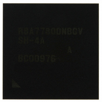
R8A77800ANBGAV Renesas Electronics America, R8A77800ANBGAV Datasheet - Page 372

R8A77800ANBGAV
Manufacturer Part Number
R8A77800ANBGAV
Description
IC SUPERH MPU ROMLESS 449-BGA
Manufacturer
Renesas Electronics America
Series
SuperH® SH7780r
Datasheet
1.R8A77800ANBGV.pdf
(1342 pages)
Specifications of R8A77800ANBGAV
Core Processor
SH-4A
Core Size
32-Bit
Speed
400MHz
Connectivity
Audio Codec, MMC, Serial Sound, SCI, SIO, SPI, SSI
Peripherals
DMA, POR, WDT
Number Of I /o
75
Program Memory Type
ROMless
Ram Size
16K x 8
Voltage - Supply (vcc/vdd)
1.15 V ~ 1.35 V
Oscillator Type
External
Operating Temperature
-20°C ~ 75°C
Package / Case
449-BGA
Lead Free Status / RoHS Status
Lead free / RoHS Compliant
Eeprom Size
-
Program Memory Size
-
Data Converters
-
Available stocks
Company
Part Number
Manufacturer
Quantity
Price
Company:
Part Number:
R8A77800ANBGAV
Manufacturer:
Renesas Electronics America
Quantity:
10 000
- Current page: 372 of 1342
- Download datasheet (7Mb)
Section 11 Local Bus State Controller (LBSC)
11.3
11.3.1
The architecture of this LSI provides a 32-bit address space. The virtual address space is divided
into five areas (P0 to P4 areas) according to the upper address value.
This LSI supports both a 29-bit and a 32-bit physical address space, and the LBSC supports a 29-
bit physical address space. The 29-bit physical address space is divided into eight areas (areas 0 to
7) according to the upper three bits [28:26] of an address and the LBSC can control areas 0 to 2
and 4 to 6 as an external memory space. The maximum capacity of each area used as an external
memory space is 64 Mbytes; the LBSC can control a total of 6 areas with a maximum capacity of
384 Mbytes as the external memory spaces.
A virtual address can be allocated to any physical address through the address translation function
of the MMU. For details, see section 7, Memory Management Unit (MMU).
With the LBSC, various types of memory or PC cards can be connected to each of the six areas as
shown in table 11.2, and accordingly output the chip select signals (CS0 to CS2, CS4 to CS6,
CE2A and CE2B). CS0 to CS2 are asserted when accessing areas 0 to 2 individually, and CS4 to
CS6 are asserted when accessing areas 4 to 6 individually. When the PCMCIA interface is
selected for area 5 or 6, CE2A or CE2B is asserted along with CS5 and CS6 for the bytes to be
accessed.
Area 3 is for DDR-SDRAM memory space and controlled by the DDR-SDRAM Interface
(DDRIF). For details, see section 12, DDR-SDRAM Interface (DDRIF).
Areas 2, 4, and 5 can also be used for the DDR-SDRAM memory space, and area 4 can also be
used for the PCI memory space by setting the Memory Address Map Select Register (MMSELR).
Area 7 is a reserved area. For the PCI memory space, see section 13, PCI Controller (PCIC). Both
DDRIF and PCIC support a 32-bit physical address space in addition to a 29-bit address. For a 32-
bit physical address, refer also to section 7.7, 32-Bit Address Extended mode.
Rev.1.00 Dec. 13, 2005 Page 320 of 1286
REJ09B0158-0100
Area Overview
Space Divisions
Related parts for R8A77800ANBGAV
Image
Part Number
Description
Manufacturer
Datasheet
Request
R

Part Number:
Description:
KIT STARTER FOR M16C/29
Manufacturer:
Renesas Electronics America
Datasheet:

Part Number:
Description:
KIT STARTER FOR R8C/2D
Manufacturer:
Renesas Electronics America
Datasheet:

Part Number:
Description:
R0K33062P STARTER KIT
Manufacturer:
Renesas Electronics America
Datasheet:

Part Number:
Description:
KIT STARTER FOR R8C/23 E8A
Manufacturer:
Renesas Electronics America
Datasheet:

Part Number:
Description:
KIT STARTER FOR R8C/25
Manufacturer:
Renesas Electronics America
Datasheet:

Part Number:
Description:
KIT STARTER H8S2456 SHARPE DSPLY
Manufacturer:
Renesas Electronics America
Datasheet:

Part Number:
Description:
KIT STARTER FOR R8C38C
Manufacturer:
Renesas Electronics America
Datasheet:

Part Number:
Description:
KIT STARTER FOR R8C35C
Manufacturer:
Renesas Electronics America
Datasheet:

Part Number:
Description:
KIT STARTER FOR R8CL3AC+LCD APPS
Manufacturer:
Renesas Electronics America
Datasheet:

Part Number:
Description:
KIT STARTER FOR RX610
Manufacturer:
Renesas Electronics America
Datasheet:

Part Number:
Description:
KIT STARTER FOR R32C/118
Manufacturer:
Renesas Electronics America
Datasheet:

Part Number:
Description:
KIT DEV RSK-R8C/26-29
Manufacturer:
Renesas Electronics America
Datasheet:

Part Number:
Description:
KIT STARTER FOR SH7124
Manufacturer:
Renesas Electronics America
Datasheet:

Part Number:
Description:
KIT STARTER FOR H8SX/1622
Manufacturer:
Renesas Electronics America
Datasheet:

Part Number:
Description:
KIT DEV FOR SH7203
Manufacturer:
Renesas Electronics America
Datasheet:


