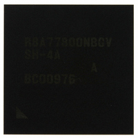
R8A77800ANBGAV Renesas Electronics America, R8A77800ANBGAV Datasheet - Page 33

R8A77800ANBGAV
Manufacturer Part Number
R8A77800ANBGAV
Description
IC SUPERH MPU ROMLESS 449-BGA
Manufacturer
Renesas Electronics America
Series
SuperH® SH7780r
Datasheet
1.R8A77800ANBGV.pdf
(1342 pages)
Specifications of R8A77800ANBGAV
Core Processor
SH-4A
Core Size
32-Bit
Speed
400MHz
Connectivity
Audio Codec, MMC, Serial Sound, SCI, SIO, SPI, SSI
Peripherals
DMA, POR, WDT
Number Of I /o
75
Program Memory Type
ROMless
Ram Size
16K x 8
Voltage - Supply (vcc/vdd)
1.15 V ~ 1.35 V
Oscillator Type
External
Operating Temperature
-20°C ~ 75°C
Package / Case
449-BGA
Lead Free Status / RoHS Status
Lead free / RoHS Compliant
Eeprom Size
-
Program Memory Size
-
Data Converters
-
Available stocks
Company
Part Number
Manufacturer
Quantity
Price
Company:
Part Number:
R8A77800ANBGAV
Manufacturer:
Renesas Electronics America
Quantity:
10 000
- Current page: 33 of 1342
- Download datasheet (7Mb)
Figure 11.2 Correspondence between Virtual Address Space and External Memory
Figure 11.3 External Memory Space Allocation (29-bit address mode)..................................... 323
Figure 11.4 Basic Timing of SRAM Interface............................................................................ 362
Figure 11.5 Example of 32-Bit Data-Width SRAM Connection ................................................ 363
Figure 11.6 Example of 16-Bit Data-Width SRAM Connection ................................................ 364
Figure 11.7 Example of 8-Bit Data-Width SRAM Connection .................................................. 365
Figure 11.8 SRAM Interface Wait Timing (Software Wait Only) ............................................. 366
Figure 11.9 SRAM Interface Wait Timing
Figure 11.10 SRAM Interface Wait Timing (Read-Strobe Negate Timing Setting) .................. 369
Figure 11.11 Burst ROM Basic Timing...................................................................................... 371
Figure 11.12 Burst ROM Wait Timing....................................................................................... 371
Figure 11.13 Burst ROM Wait Timing....................................................................................... 372
Figure 11.14 CExx and DACK Output of ATA Complement Mode in DMA Transfer............. 374
Figure 11.15 Example of PCMCIA Interface ............................................................................. 377
Figure 11.16 Basic Timing for PCMCIA Memory Card Interface ............................................. 378
Figure 11.17 Wait Timing for PCMCIA Memory Card Interface .............................................. 379
Figure 11.18 Basic Timing for PCMCIA I/O Card Interface ..................................................... 380
Figure 11.19 Wait Timing for PCMCIA I/O Card Interface ...................................................... 381
Figure 11.20 Dynamic Bus Sizing Timing for PCMCIA I/O Card Interface ............................. 382
Figure 11.21 Example of 32-Bit Data Width MPX Connection ................................................. 384
Figure 11.22 MPX Interface Timing 1 (Single Read Cycle, IW = 0, No External Wait) ........... 384
Figure 11.23 MPX Interface Timing 2 (Single Read, IW = 0, One External Wait Inserted)...... 385
Figure 11.24 MPX Interface Timing 3 (Single Write Cycle, IW = 0, No External Wait) .......... 385
Figure 11.25 MPX Interface Timing 4
Figure 11.26 MPX Interface Timing 5
Figure 11.27 MPX Interface Timing 6
Figure 11.28 MPX Interface Timing 7
Figure 11.29 MPX Interface Timing 8
Figure 11.30 Example of 32-Bit Data-Width Byte-Control SRAM ........................................... 389
Figure 11.31 Byte-Control SRAM Basic Read Cycle (No Wait) ............................................... 390
Figure 11.32 Byte-Control SRAM Basic Read Cycle (One Internal Wait Cycle)...................... 391
Figure 11.33 Byte-Control SRAM Basic Read Cycle
Space of LBSC........................................................................................................ 321
(Wait Cycle Insertion by RDY Signal, RDY Signal is synchronous input) ............ 367
(One Internal Wait + One External Wait).............................................................. 392
(Single Write Cycle, IW = 1, One External Wait Inserted).................................. 386
(Burst Read Cycle, IW = 0, No External Wait, 32-Byte Data Transfer) ............... 386
(Burst Read Cycle, IW = 0, External Wait Control, 32-Byte Data Transfer)........ 387
(Burst Write Cycle, IW = 0, No External Wait, 32-Byte Data Transfer) .............. 387
(Burst Write Cycle, IW = 1, External Wait Control, 32-Byte Data Transfer) ....... 388
Rev.1.00 Dec. 13, 2005 Page xxxi of l
Related parts for R8A77800ANBGAV
Image
Part Number
Description
Manufacturer
Datasheet
Request
R

Part Number:
Description:
KIT STARTER FOR M16C/29
Manufacturer:
Renesas Electronics America
Datasheet:

Part Number:
Description:
KIT STARTER FOR R8C/2D
Manufacturer:
Renesas Electronics America
Datasheet:

Part Number:
Description:
R0K33062P STARTER KIT
Manufacturer:
Renesas Electronics America
Datasheet:

Part Number:
Description:
KIT STARTER FOR R8C/23 E8A
Manufacturer:
Renesas Electronics America
Datasheet:

Part Number:
Description:
KIT STARTER FOR R8C/25
Manufacturer:
Renesas Electronics America
Datasheet:

Part Number:
Description:
KIT STARTER H8S2456 SHARPE DSPLY
Manufacturer:
Renesas Electronics America
Datasheet:

Part Number:
Description:
KIT STARTER FOR R8C38C
Manufacturer:
Renesas Electronics America
Datasheet:

Part Number:
Description:
KIT STARTER FOR R8C35C
Manufacturer:
Renesas Electronics America
Datasheet:

Part Number:
Description:
KIT STARTER FOR R8CL3AC+LCD APPS
Manufacturer:
Renesas Electronics America
Datasheet:

Part Number:
Description:
KIT STARTER FOR RX610
Manufacturer:
Renesas Electronics America
Datasheet:

Part Number:
Description:
KIT STARTER FOR R32C/118
Manufacturer:
Renesas Electronics America
Datasheet:

Part Number:
Description:
KIT DEV RSK-R8C/26-29
Manufacturer:
Renesas Electronics America
Datasheet:

Part Number:
Description:
KIT STARTER FOR SH7124
Manufacturer:
Renesas Electronics America
Datasheet:

Part Number:
Description:
KIT STARTER FOR H8SX/1622
Manufacturer:
Renesas Electronics America
Datasheet:

Part Number:
Description:
KIT DEV FOR SH7203
Manufacturer:
Renesas Electronics America
Datasheet:


