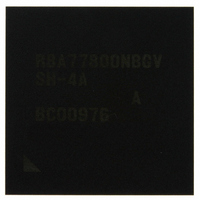
R8A77800ANBGAV Renesas Electronics America, R8A77800ANBGAV Datasheet - Page 498

R8A77800ANBGAV
Manufacturer Part Number
R8A77800ANBGAV
Description
IC SUPERH MPU ROMLESS 449-BGA
Manufacturer
Renesas Electronics America
Series
SuperH® SH7780r
Datasheet
1.R8A77800ANBGV.pdf
(1342 pages)
Specifications of R8A77800ANBGAV
Core Processor
SH-4A
Core Size
32-Bit
Speed
400MHz
Connectivity
Audio Codec, MMC, Serial Sound, SCI, SIO, SPI, SSI
Peripherals
DMA, POR, WDT
Number Of I /o
75
Program Memory Type
ROMless
Ram Size
16K x 8
Voltage - Supply (vcc/vdd)
1.15 V ~ 1.35 V
Oscillator Type
External
Operating Temperature
-20°C ~ 75°C
Package / Case
449-BGA
Lead Free Status / RoHS Status
Lead free / RoHS Compliant
Eeprom Size
-
Program Memory Size
-
Data Converters
-
Available stocks
Company
Part Number
Manufacturer
Quantity
Price
Company:
Part Number:
R8A77800ANBGAV
Manufacturer:
Renesas Electronics America
Quantity:
10 000
- Current page: 498 of 1342
- Download datasheet (7Mb)
Section 13 PCI Controller (PCIC)
13.2
Table 13.1 shows the pin configuration of the PCIC.
Table 13.1 Input/Output Pins
Rev.1.00 Dec. 13, 2005 Page 446 of 1286
REJ09B0158-0100
Pin Name
AD31 to AD0*
CBE3 to CBE0 C/BE[3:0]
PAR
PCICLK
PCIFRAME
TRDY
IRDY
STOP
LOCK
Input/Output Pins
1
PCI standard
signal name
AD[31:0]
PAR
CLK
FRAME
TRDY
IRDY
STOP
LOCK
I/O
I/O
(TRI)
I/O
(TRI)
I/O
(TRI)
Input
I/O
(STRI)
I/O
(STRI)
I/O
(STRI)
I/O
(STRI)
I/O
(STRI)
Description
PCI Address/Data Bus
Address and data buses are multiplexed. Each bus
transaction consists of an address phase followed by
one or more data phases.
PCI Command/Byte Enable
Bus command and byte enables are multiplexed.
These signals indicate the type of transaction during
the address phase and the byte enables during the
data phases.
PCI Parity
Generates/checks even parity across AD[31:0] and
CBE[3:0].
PCI Clock
Provides timing for all transactions on the PCI bus.
PCI Frame
Current initiator drives this signal, which indicates the
start and duration or end of a transaction.
PCI Target Ready
Selected target drives this signal, which indicates the
target is ready to execute a transaction. During a write,
this signal indicates that the target is ready to accept
data. During a read, this signal indicates that valid data
is present on the AD [31:0] lines.
PCI Initiator Ready
The current bus master drives this signal. During a
write, this signal indicates that valid data is present on
the AD [31:0] lines. During a read, this signal indicates
that the master is ready to accept data.
PCI Stop
Selected target drives this signal to stop the current
transaction.
PCI Lock
Related parts for R8A77800ANBGAV
Image
Part Number
Description
Manufacturer
Datasheet
Request
R

Part Number:
Description:
KIT STARTER FOR M16C/29
Manufacturer:
Renesas Electronics America
Datasheet:

Part Number:
Description:
KIT STARTER FOR R8C/2D
Manufacturer:
Renesas Electronics America
Datasheet:

Part Number:
Description:
R0K33062P STARTER KIT
Manufacturer:
Renesas Electronics America
Datasheet:

Part Number:
Description:
KIT STARTER FOR R8C/23 E8A
Manufacturer:
Renesas Electronics America
Datasheet:

Part Number:
Description:
KIT STARTER FOR R8C/25
Manufacturer:
Renesas Electronics America
Datasheet:

Part Number:
Description:
KIT STARTER H8S2456 SHARPE DSPLY
Manufacturer:
Renesas Electronics America
Datasheet:

Part Number:
Description:
KIT STARTER FOR R8C38C
Manufacturer:
Renesas Electronics America
Datasheet:

Part Number:
Description:
KIT STARTER FOR R8C35C
Manufacturer:
Renesas Electronics America
Datasheet:

Part Number:
Description:
KIT STARTER FOR R8CL3AC+LCD APPS
Manufacturer:
Renesas Electronics America
Datasheet:

Part Number:
Description:
KIT STARTER FOR RX610
Manufacturer:
Renesas Electronics America
Datasheet:

Part Number:
Description:
KIT STARTER FOR R32C/118
Manufacturer:
Renesas Electronics America
Datasheet:

Part Number:
Description:
KIT DEV RSK-R8C/26-29
Manufacturer:
Renesas Electronics America
Datasheet:

Part Number:
Description:
KIT STARTER FOR SH7124
Manufacturer:
Renesas Electronics America
Datasheet:

Part Number:
Description:
KIT STARTER FOR H8SX/1622
Manufacturer:
Renesas Electronics America
Datasheet:

Part Number:
Description:
KIT DEV FOR SH7203
Manufacturer:
Renesas Electronics America
Datasheet:


