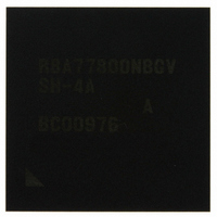
R8A77800ANBGAV Renesas Electronics America, R8A77800ANBGAV Datasheet - Page 596

R8A77800ANBGAV
Manufacturer Part Number
R8A77800ANBGAV
Description
IC SUPERH MPU ROMLESS 449-BGA
Manufacturer
Renesas Electronics America
Series
SuperH® SH7780r
Datasheet
1.R8A77800ANBGV.pdf
(1342 pages)
Specifications of R8A77800ANBGAV
Core Processor
SH-4A
Core Size
32-Bit
Speed
400MHz
Connectivity
Audio Codec, MMC, Serial Sound, SCI, SIO, SPI, SSI
Peripherals
DMA, POR, WDT
Number Of I /o
75
Program Memory Type
ROMless
Ram Size
16K x 8
Voltage - Supply (vcc/vdd)
1.15 V ~ 1.35 V
Oscillator Type
External
Operating Temperature
-20°C ~ 75°C
Package / Case
449-BGA
Lead Free Status / RoHS Status
Lead free / RoHS Compliant
Eeprom Size
-
Program Memory Size
-
Data Converters
-
Available stocks
Company
Part Number
Manufacturer
Quantity
Price
Company:
Part Number:
R8A77800ANBGAV
Manufacturer:
Renesas Electronics America
Quantity:
10 000
- Current page: 596 of 1342
- Download datasheet (7Mb)
Section 13 PCI Controller (PCIC)
The PCIC can store the error information on the PCI bus. If an error occurs, the error address is
stored in the PCI error address information register (PCIAIR), the types of transfer and command
information are stored in the PCI error command information register. And then if the PCIC
operates host bus bridge mode, the bus master information is stored in the PCI error bus master
information register.
Error information is stored only one information. This causes only to store the first occurred error
information, and not to store after second error information. The error information is initialized by
a power-on reset.
13.4.6
When operating in normal mode, the PCI bus arbitration function in the PCIC is disabled and PCI
bus arbitration is performed according to the specifications of the externally connected PCI bus
arbiter.
In normal mode, the master performs bus parking is decided by the grant signal that asserted from
the external bus arbiter. If the master that performing bus parking is different from the next
transaction master, the bus will be high-impedance state for minimum one clock cycle before the
address phase.
In normal mode, the GNT0/GNTIN pin is used for the grant input signal to the PCIC, and the
REQ0/REQOUT pin is used for the request output signal from the PCIC.
13.4.7
The PCIC supports PCI power management revision 1.1. Supported features are shown below.
• Support for the PCI power management control configuration register.
• Support for the power-down/restore request interrupts from hosts on the PCI bus.
There are seven configuration registers for PCI power management control. PCI capabilities
pointer register shows the address offset of the configuration registers for power management. In
the PCIC, this offset is fixed at CP = H'40. PCI capability ID (PCICID), next item pointer
(PCINIP), power management capability (PCIPMC), power management control/status
(PCIPMCSR), PMCSR bridge support extension (PCIPMCSRBSE) and power
consumption/dissipation (PCIPCDD) are power management registers. They support four states:
power state D0 (normal) power state D1 (bus idle) power state D2 (clock stop) and power state D3
(power down mode).
Figure 13.16 shows the PCI local bus power down state transition.
Rev.1.00 Dec. 13, 2005 Page 544 of 1286
REJ09B0158-0100
Normal mode
Power Management
Related parts for R8A77800ANBGAV
Image
Part Number
Description
Manufacturer
Datasheet
Request
R

Part Number:
Description:
KIT STARTER FOR M16C/29
Manufacturer:
Renesas Electronics America
Datasheet:

Part Number:
Description:
KIT STARTER FOR R8C/2D
Manufacturer:
Renesas Electronics America
Datasheet:

Part Number:
Description:
R0K33062P STARTER KIT
Manufacturer:
Renesas Electronics America
Datasheet:

Part Number:
Description:
KIT STARTER FOR R8C/23 E8A
Manufacturer:
Renesas Electronics America
Datasheet:

Part Number:
Description:
KIT STARTER FOR R8C/25
Manufacturer:
Renesas Electronics America
Datasheet:

Part Number:
Description:
KIT STARTER H8S2456 SHARPE DSPLY
Manufacturer:
Renesas Electronics America
Datasheet:

Part Number:
Description:
KIT STARTER FOR R8C38C
Manufacturer:
Renesas Electronics America
Datasheet:

Part Number:
Description:
KIT STARTER FOR R8C35C
Manufacturer:
Renesas Electronics America
Datasheet:

Part Number:
Description:
KIT STARTER FOR R8CL3AC+LCD APPS
Manufacturer:
Renesas Electronics America
Datasheet:

Part Number:
Description:
KIT STARTER FOR RX610
Manufacturer:
Renesas Electronics America
Datasheet:

Part Number:
Description:
KIT STARTER FOR R32C/118
Manufacturer:
Renesas Electronics America
Datasheet:

Part Number:
Description:
KIT DEV RSK-R8C/26-29
Manufacturer:
Renesas Electronics America
Datasheet:

Part Number:
Description:
KIT STARTER FOR SH7124
Manufacturer:
Renesas Electronics America
Datasheet:

Part Number:
Description:
KIT STARTER FOR H8SX/1622
Manufacturer:
Renesas Electronics America
Datasheet:

Part Number:
Description:
KIT DEV FOR SH7203
Manufacturer:
Renesas Electronics America
Datasheet:


