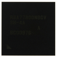
R8A77800ANBGAV Renesas Electronics America, R8A77800ANBGAV Datasheet - Page 593

R8A77800ANBGAV
Manufacturer Part Number
R8A77800ANBGAV
Description
IC SUPERH MPU ROMLESS 449-BGA
Manufacturer
Renesas Electronics America
Series
SuperH® SH7780r
Datasheet
1.R8A77800ANBGV.pdf
(1342 pages)
Specifications of R8A77800ANBGAV
Core Processor
SH-4A
Core Size
32-Bit
Speed
400MHz
Connectivity
Audio Codec, MMC, Serial Sound, SCI, SIO, SPI, SSI
Peripherals
DMA, POR, WDT
Number Of I /o
75
Program Memory Type
ROMless
Ram Size
16K x 8
Voltage - Supply (vcc/vdd)
1.15 V ~ 1.35 V
Oscillator Type
External
Operating Temperature
-20°C ~ 75°C
Package / Case
449-BGA
Lead Free Status / RoHS Status
Lead free / RoHS Compliant
Eeprom Size
-
Program Memory Size
-
Data Converters
-
Available stocks
Company
Part Number
Manufacturer
Quantity
Price
Company:
Part Number:
R8A77800ANBGAV
Manufacturer:
Renesas Electronics America
Quantity:
10 000
- Current page: 593 of 1342
- Download datasheet (7Mb)
13.4.5
(1)
The PCIC supports a subset of the PCI Local Bus Specification Revision 2.2 and can be connected
to a device with a PCI bus interface.
While the PCIC is set in host bus bridge mode, or while set in normal mode, operation differs
according to whether or not bus parking is performed, and whether or not the PCI bus arbiter
function is enabled or not.
In host bus bridge mode, the AD, CBE, PAR signal lines are driven by the PCIC when transfers
are not being performed on the PCI bus. When the PCIC subsequently starts transfers as master,
these signal lines continue to be driven until the end of the address phase.
The arbiter in the PCIC and the REQ and GNT between PCIC are connected internally. Here, pins
REQ0/REQOUT, REQ1, REQ2, and REQ3 function as the REQ inputs from the external masters
0 to 3. Similarly, GNT0/GNTIN, GNT1, GNT2, and GNT3 function as the GNT outputs to
external masters 0 to 3. Including the PCIC, arbitration of up to five masters is possible.
(2)
The PCIC supports configuration mechanism #1. The PCI PIO address register (PCIPAR) and PCI
PIO data register (PCIPDR) correspond to the configuration address register and configuration
data register, respectively.
When PCIPDR is read from or written to after PCIPAR has been set, a configuration cycle is
issued on a PCI bus.
For a type 0 transfer, bits 10 to 2 of the configuration address register are sent without translation
and bits 31 to 11 are translated so that these bits can be used as the IDSEL signal.
Bit 16 of the AD signal is driven to 1 and the other bits are made 0 by setting the device number to
0.
Bit 17 of the AD signal is driven to 1 and the other bits are made 0 by setting the device number to
1. Similarly, setting the device number to 2 drives bit 18 of the AD signal to 1 and setting the
device number to 3 drives bit 19 of the AD signal to 0.
Bit 31 of the AD signal is driven to 1 and the other bits are made 0 by setting the device number to
16.
For details, refer to "PCI Local Bus Specification Revision 2.2, section 3.2.2.3 Configuration
Space Decoding".
PCI Host bus bridge Mode Operation
Configuration Space Access
Host Bus Bridge Mode
Rev.1.00 Dec. 13, 2005 Page 541 of 1286
Section 13 PCI Controller (PCIC)
REJ09B0158-0100
Related parts for R8A77800ANBGAV
Image
Part Number
Description
Manufacturer
Datasheet
Request
R

Part Number:
Description:
KIT STARTER FOR M16C/29
Manufacturer:
Renesas Electronics America
Datasheet:

Part Number:
Description:
KIT STARTER FOR R8C/2D
Manufacturer:
Renesas Electronics America
Datasheet:

Part Number:
Description:
R0K33062P STARTER KIT
Manufacturer:
Renesas Electronics America
Datasheet:

Part Number:
Description:
KIT STARTER FOR R8C/23 E8A
Manufacturer:
Renesas Electronics America
Datasheet:

Part Number:
Description:
KIT STARTER FOR R8C/25
Manufacturer:
Renesas Electronics America
Datasheet:

Part Number:
Description:
KIT STARTER H8S2456 SHARPE DSPLY
Manufacturer:
Renesas Electronics America
Datasheet:

Part Number:
Description:
KIT STARTER FOR R8C38C
Manufacturer:
Renesas Electronics America
Datasheet:

Part Number:
Description:
KIT STARTER FOR R8C35C
Manufacturer:
Renesas Electronics America
Datasheet:

Part Number:
Description:
KIT STARTER FOR R8CL3AC+LCD APPS
Manufacturer:
Renesas Electronics America
Datasheet:

Part Number:
Description:
KIT STARTER FOR RX610
Manufacturer:
Renesas Electronics America
Datasheet:

Part Number:
Description:
KIT STARTER FOR R32C/118
Manufacturer:
Renesas Electronics America
Datasheet:

Part Number:
Description:
KIT DEV RSK-R8C/26-29
Manufacturer:
Renesas Electronics America
Datasheet:

Part Number:
Description:
KIT STARTER FOR SH7124
Manufacturer:
Renesas Electronics America
Datasheet:

Part Number:
Description:
KIT STARTER FOR H8SX/1622
Manufacturer:
Renesas Electronics America
Datasheet:

Part Number:
Description:
KIT DEV FOR SH7203
Manufacturer:
Renesas Electronics America
Datasheet:


