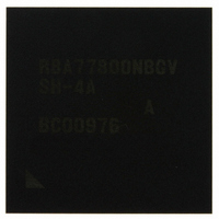
R8A77800ANBGAV Renesas Electronics America, R8A77800ANBGAV Datasheet - Page 34

R8A77800ANBGAV
Manufacturer Part Number
R8A77800ANBGAV
Description
IC SUPERH MPU ROMLESS 449-BGA
Manufacturer
Renesas Electronics America
Series
SuperH® SH7780r
Datasheet
1.R8A77800ANBGV.pdf
(1342 pages)
Specifications of R8A77800ANBGAV
Core Processor
SH-4A
Core Size
32-Bit
Speed
400MHz
Connectivity
Audio Codec, MMC, Serial Sound, SCI, SIO, SPI, SSI
Peripherals
DMA, POR, WDT
Number Of I /o
75
Program Memory Type
ROMless
Ram Size
16K x 8
Voltage - Supply (vcc/vdd)
1.15 V ~ 1.35 V
Oscillator Type
External
Operating Temperature
-20°C ~ 75°C
Package / Case
449-BGA
Lead Free Status / RoHS Status
Lead free / RoHS Compliant
Eeprom Size
-
Program Memory Size
-
Data Converters
-
Available stocks
Company
Part Number
Manufacturer
Quantity
Price
Company:
Part Number:
R8A77800ANBGAV
Manufacturer:
Renesas Electronics America
Quantity:
10 000
- Current page: 34 of 1342
- Download datasheet (7Mb)
Figure 11.34 Wait Cycles between Access Cycles ..................................................................... 394
Figure 11.35 Arbitration Sequence............................................................................................. 396
Figure 11.36 Example of the Bus Release Restraint by the DMAC CHCR LCKN bit .............. 398
Section 12 DDR-SDRAM Interface (DDRIF)
Figure 12.1 DDRIF Block Diagram ........................................................................................... 402
Figure 12.2 Physical Address Space of This LSI ....................................................................... 405
Figure 12.3 Data Alignment in DDR-SDRAM and DDRIF....................................................... 409
Figure 12.4 Relationship between Write Values in SDMR and
Figure 12.5 DDRIF Basic Timing
Figure 12.6 DDRIF Basic Timing
Figure 12.7 DDRIF Basic Timing (1-/2-/4-/8-Byte Single Burst Read with Auto Precharge)... 432
Figure 12.8 DDRIF Basic Timing
Figure 12.9 DDRIF Basic Timing (4 Burst Read: 32-byte without Auto Precharge)................. 434
Figure 12.10 DDRIF Basic Timing (4 Burst Write: 32-byte without Auto Precharge).............. 435
Figure 12.11 DDRIF Basic Timing (from Precharging All Banks to Bank Activation)............. 436
Figure 12.12 DDRIF Basic Timing (Mode Register Setting)..................................................... 437
Figure 12.13 DDRIF Basic Timing (Enter Auto-Refresh/Exit to Bank Activation)................... 438
Figure 12.14 DDRIF Basic Timing (Enter Self-Refresh/Exit to Command Issuing) ................. 439
Section 13 PCI Controller (PCIC)
Figure 13.1 PCIC Block Diagram .............................................................................................. 445
Figure 13.2 SuperHyway Bus to PCI Local Bus Access ............................................................ 525
Figure 13.3 SuperHyway Bus to PCI Local Bus Address Translation
Figure 13.4 SuperHyway Bus to PCI Local Bus Address Translation
Figure 13.5 SuperHyway Bus to PCI Local Bus Address Translation
Figure 13.6 SuperHyway Bus to PCI Local Bus Address Translation (PCI I/O) ....................... 528
Figure 13.7 Endian Conversion from SuperHyway Bus to PCI Local bus
Figure 13.8 Endian Conversion from SuperHyway Bus to PCI Local bus
Figure 13.9 PCI local bus to SuperHyway bus Memory Map .................................................... 532
Figure 13.10 PCI Local Bus to SuperHyway Bus Address Translation
Rev.1.00 Dec. 13, 2005 Page xxxii of l
Output Signals to Memory Pins .............................................................................. 423
(1-/2-/4-/8-Byte Single Burst Read without Auto Precharge) ................................. 430
(1-/2-/4-/8-Byte Single Burst Write without Auto Precharge) ................................ 431
(Non-Byte Swapping: TBS = 0) .............................................................................. 530
(1-/2-/4-/8-Byte Single Burst Write with Auto Precharge) ..................................... 433
(PCI Memory Space 2)............................................................................................ 527
(Byte Swapping: TBS = 1)...................................................................................... 531
(PCI Memory Space 0) ........................................................................................... 526
(PCI Memory Space 1) ........................................................................................... 527
(Local Address Space 0/1)..................................................................................... 534
Related parts for R8A77800ANBGAV
Image
Part Number
Description
Manufacturer
Datasheet
Request
R

Part Number:
Description:
KIT STARTER FOR M16C/29
Manufacturer:
Renesas Electronics America
Datasheet:

Part Number:
Description:
KIT STARTER FOR R8C/2D
Manufacturer:
Renesas Electronics America
Datasheet:

Part Number:
Description:
R0K33062P STARTER KIT
Manufacturer:
Renesas Electronics America
Datasheet:

Part Number:
Description:
KIT STARTER FOR R8C/23 E8A
Manufacturer:
Renesas Electronics America
Datasheet:

Part Number:
Description:
KIT STARTER FOR R8C/25
Manufacturer:
Renesas Electronics America
Datasheet:

Part Number:
Description:
KIT STARTER H8S2456 SHARPE DSPLY
Manufacturer:
Renesas Electronics America
Datasheet:

Part Number:
Description:
KIT STARTER FOR R8C38C
Manufacturer:
Renesas Electronics America
Datasheet:

Part Number:
Description:
KIT STARTER FOR R8C35C
Manufacturer:
Renesas Electronics America
Datasheet:

Part Number:
Description:
KIT STARTER FOR R8CL3AC+LCD APPS
Manufacturer:
Renesas Electronics America
Datasheet:

Part Number:
Description:
KIT STARTER FOR RX610
Manufacturer:
Renesas Electronics America
Datasheet:

Part Number:
Description:
KIT STARTER FOR R32C/118
Manufacturer:
Renesas Electronics America
Datasheet:

Part Number:
Description:
KIT DEV RSK-R8C/26-29
Manufacturer:
Renesas Electronics America
Datasheet:

Part Number:
Description:
KIT STARTER FOR SH7124
Manufacturer:
Renesas Electronics America
Datasheet:

Part Number:
Description:
KIT STARTER FOR H8SX/1622
Manufacturer:
Renesas Electronics America
Datasheet:

Part Number:
Description:
KIT DEV FOR SH7203
Manufacturer:
Renesas Electronics America
Datasheet:


