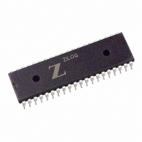
Z0847006PSG Zilog, Z0847006PSG Datasheet - Page 108

Z0847006PSG
Manufacturer Part Number
Z0847006PSG
Description
IC 6MHZ Z80 NMOS DART 40-DIP
Manufacturer
Zilog
Series
Z80r
Datasheet
1.Z0847006PSG.pdf
(330 pages)
Specifications of Z0847006PSG
Processor Type
Z80
Features
Dual Channel Asynchronous Receiver/Transmitter (DART)
Speed
6MHz
Voltage
5V
Mounting Type
Through Hole
Package / Case
40-DIP (0.620", 15.75mm)
Mounting Style
Through Hole
Cpu Speed
6MHz
Digital Ic Case Style
DIP
No. Of Pins
40
Supply Voltage Range
5V
Operating Temperature Range
0°C To +70°C
Svhc
No SVHC (18-Jun-2010)
Base Number
847006
Rohs Compliant
Yes
Clock Frequency
6MHz
Lead Free Status / RoHS Status
Lead free / RoHS Compliant
Available stocks
Company
Part Number
Manufacturer
Quantity
Price
Company:
Part Number:
Z0847006PSG
Manufacturer:
Zilog
Quantity:
22
- Current page: 108 of 330
- Download datasheet (3Mb)
PROGRAMMING
UM008101-0601
< % 2 7 2 G T K R J G T C N U
7 U G T / C P W C N
Overview
Figure 38.
The DMA must be programmed before use. Its control registers have no
useful default values at power-up. In addition, commands are frequently
written to the DMA after the initial power-up programming sets basic
DMA operating modes; this is most commonly done within service
routines for purposes such as reading status, changing starting addresses,
and reenabling both interrupt and bus-request logic after a block transfer
or search.
The DMA has two primary states that can be set: (1) an enabled state, in
which the DMA gains control of the system buses and directs data
transfers between ports or data searching from a single port; and (2) a
disabled state, in which the DMA initiates neither bus requests nor data
transfers. Table 13 describes these states and their substates in detail.
When the DMA is powered-up or reset by any means, it is automatically
placed into the disabled state. Program commands can be written to it by
the CPU in the enable/inactive state, but this automatically puts the DMA
into the disabled state, which is maintained until an ENABLE DMA
command is written by the CPU to the DMA’s Write Register 6 (WR6).
In the Z80 Family, the DMA normally exists as a peripheral device in
system I/O space. Its Chip Enable (CE) signal is decoded from the lower
byte of the address bus for this purpose and all control bytes and status
bytes are written to and read from the same I/O port address, using an
output instruction such as OTIR (in the Z80 CPU).
It is possible to use the DMA in memory mapped I/O structures, but this
involves some external logic, which is explained in the “Applications”
Polling for a Service Request Bit
Direct Memory Access
Related parts for Z0847006PSG
Image
Part Number
Description
Manufacturer
Datasheet
Request
R

Part Number:
Description:
Customer Procurement Spec(CPS)
Manufacturer:
ZILOG [Zilog, Inc.]
Datasheet:

Part Number:
Description:
Communication Controllers, ZILOG INTELLIGENT PERIPHERAL CONTROLLER (ZIP)
Manufacturer:
Zilog, Inc.
Datasheet:

Part Number:
Description:
KIT DEV FOR Z8 ENCORE 16K TO 64K
Manufacturer:
Zilog
Datasheet:

Part Number:
Description:
KIT DEV Z8 ENCORE XP 28-PIN
Manufacturer:
Zilog
Datasheet:

Part Number:
Description:
DEV KIT FOR Z8 ENCORE 8K/4K
Manufacturer:
Zilog
Datasheet:

Part Number:
Description:
KIT DEV Z8 ENCORE XP 28-PIN
Manufacturer:
Zilog
Datasheet:

Part Number:
Description:
DEV KIT FOR Z8 ENCORE 4K TO 8K
Manufacturer:
Zilog
Datasheet:

Part Number:
Description:
CMOS Z8 microcontroller. ROM 16 Kbytes, RAM 256 bytes, speed 16 MHz, 32 lines I/O, 3.0V to 5.5V
Manufacturer:
Zilog, Inc.
Datasheet:

Part Number:
Description:
Low-cost microcontroller. 512 bytes ROM, 61 bytes RAM, 8 MHz
Manufacturer:
Zilog, Inc.
Datasheet:

Part Number:
Description:
Z8 4K OTP Microcontroller
Manufacturer:
Zilog, Inc.
Datasheet:

Part Number:
Description:
CMOS SUPER8 ROMLESS MCU
Manufacturer:
Zilog, Inc.
Datasheet:

Part Number:
Description:
SL1866 CMOSZ8 OTP Microcontroller
Manufacturer:
Zilog, Inc.
Datasheet:

Part Number:
Description:
SL1866 CMOSZ8 OTP Microcontroller
Manufacturer:
Zilog, Inc.
Datasheet:

Part Number:
Description:
OTP (KB) = 1, RAM = 125, Speed = 12, I/O = 14, 8-bit Timers = 2, Comm Interfaces Other Features = Por, LV Protect, Voltage = 4.5-5.5V
Manufacturer:
Zilog, Inc.
Datasheet:


